74HC4051-Q100; 74HCT4051-Q100
NXP Semiconductors
8-channel analog multiplexer/demultiplexer
6. Pinning information
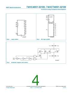
6.1 Pinning
74HC4051-Q100
74HCT4051-Q100
terminal 1
index area
74HC4051-Q100
74HCT4051-Q100
2
3
4
5
6
7
15
14
13
12
11
10
Y6
Z
Y2
Y1
Y0
Y3
S0
S1
1
2
3
4
5
6
7
8
16
15
14
13
12
11
10
9
Y4
Y6
Z
V
CC
Y7
Y5
E
Y2
Y1
Y0
Y3
S0
S1
S2
Y7
Y5
E
(1)
CC
V
V
EE
V
EE
aaa-003161
GND
Transparent top view
aaa-003160
(1) This is not a supply pin. The substrate is attached to this
pad using conductive die attach material. There is no
electrical or mechanical requirement to solder this pad.
However, if it is soldered, the solder land should remain
floating or be connected to VCC.
Fig 5. Pin configuration SO16 and TSSOP16
Fig 6. Pin configuration DHVQFN16
6.2 Pin description
Table 2.
Symbol
E
Pin description
Pin
Description
6
enable input (active LOW)
supply voltage
VEE
7
GND
8
ground supply voltage
select input
S0, S1, S2
11, 10, 9
Y0, Y1, Y2, Y3, Y4, Y5, Y6, Y7 13, 14, 15, 12, 1, 5, 2, 4 independent input or output
Z
3
common output or input
supply voltage
VCC
16
74HC_HCT4051_Q100
All information provided in this document is subject to legal disclaimers.
© NXP B.V. 2012. All rights reserved.
Product data sheet
Rev. 2 — 8 October 2012
5 of 31

 NXP [ NXP ]