74HC165-Q100; 74HCT165-Q100
NXP Semiconductors
8-bit parallel-in/serial out shift register
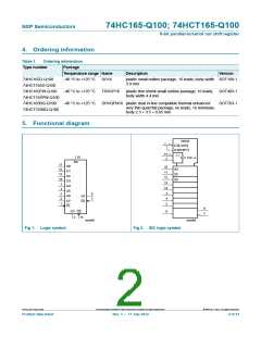
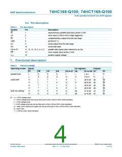
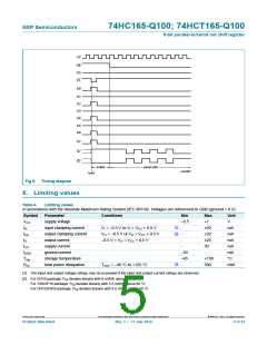
CP
CE
DS
PL
D0
D1
D2
D3
D4
D5
D6
D7
Q7
Q7
inhibit
serial shift
mna993
load
Fig 6. Timing diagram
8. Limiting values
Table 4.
Limiting values
In accordance with the Absolute Maximum Rating System (IEC 60134). Voltages are referenced to GND (ground = 0 V)
Symbol
VCC
IIK
Parameter
Conditions
Min
Max
+7
Unit
V
supply voltage
0.5
[1]
[1]
input clamping current
output clamping current
output current
VI < 0.5 V or VI > VCC + 0.5 V
VO < 0.5 V or VO > VCC + 0.5 V
0.5 V < VO < VCC + 0.5 V
-
20
20
25
50
mA
mA
mA
mA
mA
C
IOK
-
IO
-
ICC
supply current
-
IGND
Tstg
Ptot
ground current
50
65
-
-
storage temperature
total power dissipation
+150
500
[2]
Tamb = 40 C to +125 C
mW
[1] The input and output voltage ratings may be exceeded if the input and output current ratings are observed.
[2] For SO16 package: Ptot derates linearly with 8 mW/K above 70 C.
For TSSOP16 package: Ptot derates linearly with 5.5 mW/K above 60 C.
For DHVQFN16 package: Ptot derates linearly with 4.5 mW/K above 60 C.
74HC_HCT165_Q100
All information provided in this document is subject to legal disclaimers.
© NXP B.V. 2012. All rights reserved.
Product data sheet
Rev. 1 — 17 July 2012
5 of 21

 NXP [ NXP ]