74HC165-Q100; 74HCT165-Q100
NXP Semiconductors
8-bit parallel-in/serial out shift register
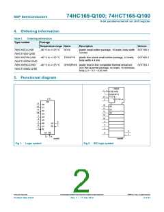
11 12 13 14 3
4
5
6
D0 D1 D2 D3 D4 D5 D6 D7
1
PL
10 DS
Q7
Q7
9
7
8-BIT SHIFT REGISTER
PARALLEL-IN/SERIAL-OUT
2
CP
15 CE
mna992
Fig 3. Functional diagram
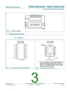
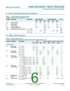
6. Pinning information
6.1 Pinning
74HC165-Q100
74HCT165-Q100
74HC165-Q100
74HCT165-Q100
terminal 1
index area
1
2
3
4
5
6
7
8
16
15
14
13
12
11
10
9
PL
CP
V
CC
CE
D3
D2
D1
D0
DS
Q7
2
15
14
13
12
11
10
CP
CE
D3
D2
D1
D0
DS
D4
3
4
5
6
7
D4
D5
D6
D7
Q7
D5
D6
(1)
GND
D7
Q7
aaa-003156
GND
Transparent top view
aaa-003155
(1) This is not a supply pin. The substrate is attached to this
pad using conductive die attach material. There is no
electrical or mechanical requirement to solder this pad.
However, if it is soldered, the solder land should remain
floating or be connected to GND.
Fig 4. Pin configuration SO16 and TSSOP16
Fig 5. Pin configuration DHVQFN16
74HC_HCT165_Q100
All information provided in this document is subject to legal disclaimers.
© NXP B.V. 2012. All rights reserved.
Product data sheet
Rev. 1 — 17 July 2012
3 of 21

 NXP [ NXP ]