74HC165-Q100; 74HCT165-Q100
NXP Semiconductors
8-bit parallel-in/serial out shift register
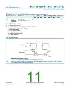
V
I
V
M
PL input
GND
t
t
rec
W
V
I
CE, CP input
V
M
GND
t
PHL
V
OH
V
Q7 or Q7 output
M
V
OL
mna988
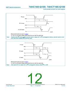
Measurement points are given in Table 8.
OL and VOH are typical voltage output levels that occur with the output load.
V
Fig 8. Parallel load (PL) pulse width, parallel load to output (Q7 or Q7) propagation delays, parallel load to clock
(CP) and clock enable (CE) recovery time
V
I
V
D7 input
M
GND
t
t
t
t
PLH
PHL
PHL
PLH
V
OH
V
V
Q7 output
Q7 output
M
M
V
OL
V
OH
V
OL
mna989
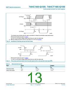
Measurement points are given in Table 8.
OL and VOH are typical voltage output levels that occur with the output load.
V
Fig 9. Data input (D7) to output (Q7 or Q7) propagation delays when PL is LOW
74HC_HCT165_Q100
All information provided in this document is subject to legal disclaimers.
© NXP B.V. 2012. All rights reserved.
Product data sheet
Rev. 1 — 17 July 2012
12 of 21

 NXP [ NXP ]