74HC165-Q100; 74HCT165-Q100
NXP Semiconductors
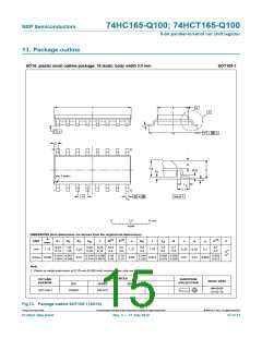
8-bit parallel-in/serial out shift register
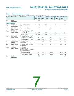
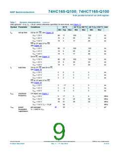
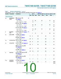
Table 7.
Dynamic characteristics …continued
GND (ground = 0 V); CL = 50 pF unless otherwise specified; for test circuit, see Figure 12
Symbol Parameter
Conditions
25 C
40 C to +85 C 40 C to +125 C Unit
Min Typ Max
Min
Max
Min
Max
[3]
CPD
power
per package;
-
35
-
-
-
-
-
pF
dissipation
capacitance
VI = GND to VCC 1.5 V
[1] tpd is the same as tPHL and tPLH
.
[2] tt is the same as tTHL and tTLH
.
[3] CPD is used to determine the dynamic power dissipation (PD in W).
PD = CPD VCC2 fi + (CL VCC2 fo) where:
fi = input frequency in MHz;
fo = output frequency in MHz;
(CL VCC2 fo) = sum of outputs;
CL = output load capacitance in pF;
VCC = supply voltage in V.
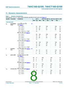
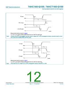
12. Waveforms
1/f
max
V
I
CP or CE input
V
M
t
GND
t
W
t
PHL
PLH
V
OH
90 %
90 %
V
M
Q7 or Q7 output
10 %
10 %
TLH
V
OL
t
t
THL
mna987
Measurement points are given in Table 8.
VOL and VOH are typical voltage output levels that occur with the output load.
Fig 7. Clock (CP) or clock enable (CE) to output (Q7 or Q7) propagation delays, clock pulse width, maximum
clock frequency and output transition times
74HC_HCT165_Q100
All information provided in this document is subject to legal disclaimers.
© NXP B.V. 2012. All rights reserved.
Product data sheet
Rev. 1 — 17 July 2012
11 of 21

 NXP [ NXP ]