Philips Semiconductors
Product specification
Hex inverting Schmitt trigger
74HC14; 74HCT14
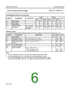
RECOMMENDED OPERATING CONDITIONS
74HC14
TYP. MAX. MIN.
74HCT14
UNIT
SYMBOL
PARAMETER
supply voltage
CONDITIONS
MIN.
2.0
TYP. MAX.
VCC
VI
5.0
−
6.0
4.5
0
5.0
5.5
V
input voltage
0
VCC
VCC
+85
−
VCC
VCC
+85
V
VO
output voltage
0
−
0
−
V
Tamb
operating ambient
temperature
see DC and AC
characteristics
per device
−40
−40
+25
−
−40
+25
−
°C
+125 −40
+125 °C
LIMITING VALUES
In accordance with the Absolute Maximum System (IEC 60134); voltages are referenced to GND (ground = 0 V).
SYMBOL
PARAMETER
supply voltage
CONDITIONS
MIN. MAX. UNIT
VCC
IIK
−0.5
+7
V
input diode current
output diode current
VI < −0.5 V or VI > VCC + 0.5 V
VO < −0.5 V or VO > VCC + 0.5 V
−0.5 V < VO < VCC + 0.5 V
−
−
−
±20
±20
±25
mA
mA
mA
IOK
IO
output source or sink
current
ICC; IGND VCC or GND current
−
50
mA
Tstg
Ptot
storage temperature
power dissipation
−65
+150 °C
Tamb = −40 to +125 °C
DIP14 packages; note 1
Other packages; note 2
−
−
750
500
mW
mW
Notes
1. For DIP14 packages: above 70 °C the value of PD derates linearly with 12 mW/K.
2. For SO14 packages: above 70 °C the value of PD derates linearly with 8 mW/K.
For (T)SSOP14 packages: above 60 °C the value of PD derates linearly with 5.5 mW/K.
For DHVQFN14 packages: above 60 °C the value of PD derates linearly with 4.5 mW/K.
2003 Oct 30
6

 NXP [ NXP ]