Philips Semiconductors
Product specification
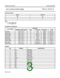
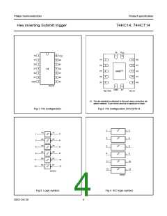
Hex inverting Schmitt trigger
74HC14; 74HCT14
FEATURES
DESCRIPTION
• Applications:
The 74HC14 and 74HCT14 are high-speed Si-gate CMOS
devices and are pin compatible with low power Schottky
TTL (LSTTL). They are specified in compliance with
JEDEC standard no. 7A.
– Wave and pulse shapers
– Astable multivibrators
– Monostable multivibrators.
• Complies with JEDEC standard no. 7A
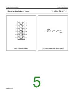
The 74HC14 and 74HCT14 provide six inverting buffers
with Schmitt-trigger action. They are capable of
transforming slowly changing input signals into sharply
defined, jitter-free output signals.
• ESD protection:
HBM EIA/JESD22-A114-A exceeds 2000 V
MM EIA/JESD22-A115-A exceeds 200 V.
• Specified from −40 to +85 °C and −40 to +125 °C.
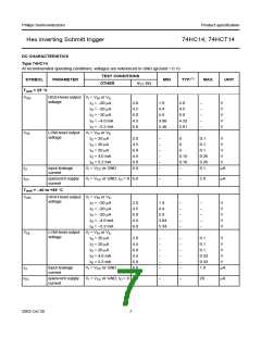
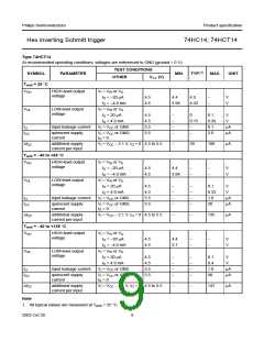
QUICK REFERENCE DATA
GND = 0 V; Tamb = 25 °C; tr = tf = 6 ns
TYPICAL
SYMBOL
PARAMETER
CONDITIONS
UNIT
HC
HCT
tPHL/tPLH
CI
propagation delay nA to nY
input capacitance
CL = 15 pF; VCC = 5 V 12
3.5
17
3.5
8
ns
pF
pF
CPD
power dissipation capacitance per gate notes 1 and 2
7
Notes
1. CPD is used to determine the dynamic power dissipation (PD in µW):
PD = CPD × VCC2 × fi × N + Σ(CL × VCC2 × fo) where:
fi = input frequency in MHz;
fo = output frequency in MHz;
CL = output load capacitance in pF;
VCC = supply voltage in Volts;
N = total load switching outputs;
Σ(CL × VCC2 × fo) = sum of the outputs.
2. For type 74HC14 the condition is VI = GND to VCC
.
For type 74HCT14 the condition is VI = GND to VCC − 1.5 V.
2003 Oct 30
2

 NXP [ NXP ]