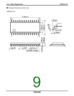
MN6761S
For Video Equipment
Pin Descriptions (continued)
Pin No.
Symbol
Pin Name
Function Description
16
VR
Vertical reset output
This pin generates a vertical reset pulse for the
V-SERATION interval detected in the GLSYNC signal.
Connect it to the VR pin of the synchronizing signal
generator.
25
26
27
SCPCO
Subcarrier phase
comparator output
This pin is at "L" level when the SC1 signal leads the
GLBSC signal and is at "H" level when the signal lags.
At all other times, it is in the high-impedance state.
Clock oscillator pins for the subcarrier circuits.
Connect these pins to a crystal oscillator, capacitor, and
variable capacitor. (The pins have built-in feedback resistors.)
The circuit oscillates during external synchronization mode.
The oscillation stops for internal synchronization mode.
The oscillator frequency, 4fSC , is 14.31818 MHz for NTSC
and 14.734 MHz for PAL.
4fSCOSCI
Oscillator input for
subcarrier circuits
4fSCOSCO Oscillator output for
subcarrier circuits
28
18
19
5
4fSC
Subcarrier clock output Clock output from subcarrier circuits.
In external synchronization mode, this pin provides the
(4fSC) clock signal; in internal synchronization mode, it
remains at "L" level. Connect this pin to the EX4fSCI pin on
the synchronizing signal generator.
LSWCONT Line switch polarity
control output
During PAL operation, this pin emits an error detection
pulse if the LSW polarity is wrong, and the chip reverses
the LSW polarity. During internal synchronization mode,
this pin remains at "L" level. Connect this pin to the
LSWCONT pin on the synchronizing signal generator.
If the chip detects GLSYNC input, it switches to external
synchronization mode and drives this pin at "H" level.
Otherwise, it switches to internal synchronization mode and
drives this pin at "L" level. Connect this pin to the EXT/INT
pin on the synchronizing signal generator.
EXT/INT
Automatic internal/
external switching
output
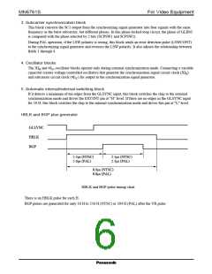
BGP
Burst gate pulse output
These pulses have a width of 2.5 µs (NTSC) or 2.3 µs
(PAL) and trail the rising edge of the HSYNC signal by
5.3 µs (NTSC) or 5.6 µs.
They are generated for only 10 H to 256 H (NTSC) or
304 H (PAL) after the VR pulse.
20
HBLK
Horizontal blanking
output
These pulses have a width of 8.9 µs (NTSC) or 8.8 µs
(PAL) and follow the rising edge of the HSYNC signal.
Leave these test inputs open. (The pins include built-in
pull-up resistors.)
21
10
TEST1
TEST2
Test inputs

 PANASONIC [ PANASONIC ]