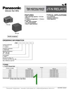
JT-N
2. 1 Form C Sealed type
Part No.
Nominal coil voltage
PCB type
TMP type
5V DC
6V DC
JTN1S-PA-F-DC5V
JTN1S-PA-F-DC6V
JTN1S-PA-F-DC9V
JTN1S-PA-F-DC12V
JTN1S-PA-F-DC15V
JTN1S-PA-F-DC18V
JTN1S-PA-F-DC24V
JTN1S-TMP-F-DC5V
JTN1S-TMP-F-DC6V
JTN1S-TMP-F-DC9V
JTN1S-TMP-F-DC12V
JTN1S-TMP-F-DC15V
JTN1S-TMP-F-DC18V
JTN1S-TMP-F-DC24V
9V DC
12V DC
15V DC
18V DC
24V DC
Standard packing: PCB type: Carton: 50 pcs.; Case: 500 pcs.
TMP type: Carton: 50 pcs.; Case: 300 pcs.
RATING
1. Coil data
Nominal operating
current
[ 10%] (at 20°C 68°F)
Nominal coil
voltage
Pick-up voltage
(at 20°C 68°F)
Drop-out voltage
(at 20°C 68°F)
Coil resistance
[ 10%] (at 20°C 68°F)
Nominal operating
power
Max. applied voltage
(at 20°C 68°F)
5V DC
6V DC
161.3mA
133.3mA
89.1mA
66.6mA
53.4mA
44.4mA
33.3mA
31Ω
45Ω
6 V
7.2V
10.8V
14.4V
9V DC
101Ω
180Ω
281Ω
405Ω
720Ω
75%V or less of
nominal voltage
(Initial)
10%V or more of
nominal voltage
(Initial)
12V DC
15V DC
18V DC
24V DC
800mW
18
V
21.6V
28.8V
2. Specifications
Characteristics
Item
Specifications
AgSnO2 type
Contact material
Arrangement
Contact resistance (Initial)
Contact
1 Form A
1 Form C
Max. 50 mΩ (By voltage drop 6 V DC 1A)
Nominal switching capacity (resistive load)
Max. switching power (resistive load)
Max. switching voltage
20A 277V AC
N.C.: 10A 277V AC, N.O.: 20A 277V AC
N.C.: 2,770VA, N.O.: 5,540VA
8,310VA (30A 277V AC)
277V AC
Rating
Max. switching current
30A
N.C.: 10A, N.O.: 20A
Nominal operating power
Min. switching capacity (reference value)*1
Approx. 800mW
100mA, 5V DC
Insulation resistance (Initial)
Min. 100MΩ (at 500V DC) Measurement at same location as “Breakdown voltage” section.
1,200 Vrms for 1 min. (Detection current: 10 mA)
Between open contacts
Between contact and coil
Breakdown voltage
(Initial)
2,500 Vrms for 1 min. (Detection current: 10 mA)
Electrical
characteristics
Surge breakdown voltage*2
(Between contact and coil) (Initial)
—
Operate time (at nominal voltage) (at 20°C 68°F)
Release time (at nominal voltage) (at 20°C 68°F)
Max. 20 ms (excluding contact bounce time.)
Max. 10 ms (excluding contact bounce time) (Without diode)
Min. 98 m/s2 (Half-wave pulse of sine wave: 11 ms; detection time: 10µs.)
Min. 980 m/s2 (Half-wave pulse of sine wave: 6 ms.)
10 to 55 Hz at double amplitude of 1.5 mm (Detection time: 10µs.)
10 to 55 Hz at double amplitude of 2 mm
Functional
Shock resistance
Destructive
Mechanical
characteristics
Functional
Vibration resistance
Destructive
Mechanical
Min. 1×10⁷
N.O.: Min. 1×10⁵
Expected life
(20A 277V AC at resistive load)
Electrical (at 20 times/min.)*3
Min. 1×10⁵ (20A 277V AC at resistive load)
N.C.: Min. 1×10⁵
(10A 277V AC at resistive load)
Ambient temperature: –55°C to +85°C –67°F to +185°F,
Conditions for operation, transport and storage*4
Max. operating speed
Humidity: 5 to 85% R.H. (Not freezing and condensing at low temperature)
Conditions
Unit weight
20 times/min. (at nominal switching capacity)
PCB type: Approx. 25 g .88 oz
TMP type: Approx. 30 g 1.06 oz
* Specifications will vary with foreign standards certification ratings.
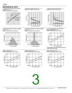
Notes: *1. This value can change due to the switching frequency, environmental conditions, and desired reliability level, therefore it is recommended to check this with the
actual load.
*2. Wave is standard shock voltage of 1.2×50µs according to JEC-212-1981
*3. In order to obtain the full rated life cycles, the relay should be properly vented by removing the vent nib. More detail, please look at caution for NOTES.
*4. The upper limit of the ambient temperature is the maximum temperature that can satisfy the coil temperature rise value. Refer to Usage, transport and storage
conditions in NOTES.
ASCTB187E 201202-T
Panasonic Corporation Automation Controls Business Unit industrial.panasonic.com/ac/e/

 PANASONIC [ PANASONIC ]