DSP
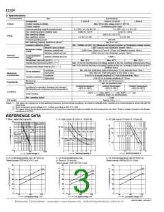
2. Specifications
Characteristics
Item
Specifications
1 Form A 1 Form B
Arrangement
1 Form A
2 Form A
Contact
Contact resistance (Initial)
Contact material
Max. 30 mΩ (By voltage drop 6 V DC 1A)
Au-flashed AgSnO2 type
Nominal switching capacity (resistive load)
Max. switching power (resistive load)
Max. switching voltage
8 A 250 V AC, 5A 30V DC
2,000 VA, 150 W
5 A 250 V AC, 5 A 30 V DC
1,250 VA, 150 W
250 V AC, 125 V DC
5 A AC, DC
Rating
Max. switching current
8 A AC, 5 A DC
Nominal operating power
300 mW
Min. switching capacity (Reference value)*1
Insulation resistance (Initial)
Between open contacts
10m A 5 V DC
Min. 1,000MΩ (at 500V DC) Measurement at same location as “Breakdown voltage” section.
1,000 Vrms for 1min. (Detection current: 10mA.)
Breakdown voltage
Between contact sets
(Initial)
2,000 Vrms (1 Form A 1 Form B, 2 Form A) (Detection current: 10mA.)
3,000 Vrms for 1min. (Detection current: 10mA.)
Between contact and coil
Electrical
characteristics
Surge breakdown
between contacts and coil
voltage*2
5,000 V
Temperature rise (coil) (at 65°C 149°F)
Operate time [Set time] (at 20°C 68°F)
Max. 55°C
Max. 40°C
Max. 55°C
Max. 10 ms [10 ms] (Nominal coil voltage applied to the coil, excluding contact bounce time.)
Max. 5 ms [10 ms] (Nominal coil voltage applied to the coil, excluding contact bounce time.)
(without diode)
Release time [Reset time] (at 20°C 68°F)
Functional
Shock resistance
Min. 196 m/s2 (Half-wave pulse of sine wave: 11 ms; detection time: 10µs.)
Min. 980 m/s2 (Half-wave pulse of sine wave: 6 ms.)
10 to 55 Hz at double amplitude of 2 mm (Detection time: 10µs.)
10 to 55 Hz at double amplitude of 3.5 mm
Destructive
Mechanical
characteristics
Functional
Vibration resistance
Destructive
Mechanical
Electrical
Min. 5×10⁷ (at 180 times/min.)
Expected life
Min. 105 (resistive load)
Ambient temperature:
–40°C to +60°C
–40°F to +140°F
Ambient temperature:
–40°C to +65°C
–40°F to +149°F
Ambient temperature:
–40°C to +60°C
–40°F to +140°F
Conditions for operation, transport and storage*3
(Not freezing and condensing at low temperature)
Conditions
Unit weight
250°C 482°F (10s), 300°C 572°F (5s), 350°C 662°F (3s)
Solder heating
(Soldering depth: 2/3 terminal pitch)
Max. operating speed
3 cps
Approx. 4.5 g .16 oz
Notes: *1. This value can change due to the switching frequency, environmental conditions, and desired reliability level, therefore it is recommended to check this with the
actual load.
*2. Wave is standard shock voltage of 1.2×50µs according to JEC-212-1981
*3. The upper limit of the ambient temperature is the maximum temperature that can satisfy the coil temperature rise value. Refer to Usage, transport and storage
conditions in NOTES.
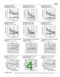
REFERENCE DATA
1. Max. switching capacity
2.-(1) Life curve (1 Form A 1 Form B)
2.-(2) Life curve (1 Form A 1 Form B)
10
AC resistive
load (1a)
100
100
30 V DC resistive
AC resistive
load
265 V·130 V AC cosϕ = 1
(1a1b,2a)
50
DC resistive
load (1a)
30 V DC L/R = 7 ms
1
10
265 V·130 V AC
cosϕ = 0.4
DC resistive load
(1a1b,2a)
10
0.1
0.5
1
5
10
0
1
2
3
4
5
6
7
10
100
1000
Switching capacity, A
Switching capacity, A
Contact voltage, V
3.-(1) Coil temperature rise (1 Form A)
Tested sample: DSP1a-DC12V, 5 pcs.
3.-(2) Coil temperature rise
(1 Form A 1 Form B)
3.-(3) Coil temperature rise (2 Form A)
Tested sample: DSP2a-DC12V, 5 pcs.
Tested sample: DSP1-DC12V, 5 pcs.
60
60
60
5A
8A
0A
50
40
30
20
10
0
50
50
5A
0A
0A
40
40
30
20
10
0
30
20
10
0
80
100
120
80
100
120
80
100
120
Coil applied voltage, %V
Coil applied voltage, %V
Coil applied voltage, %V
ASCTB180E 201202-T
Panasonic Corporation Automation Controls Business Unit industrial.panasonic.com/ac/e/

 PANASONIC [ PANASONIC ]