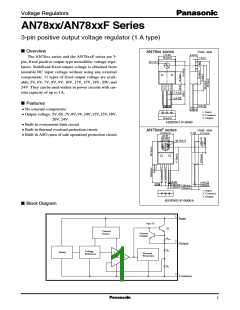
AN78xx/AN78xxF Series
Voltage Regulators
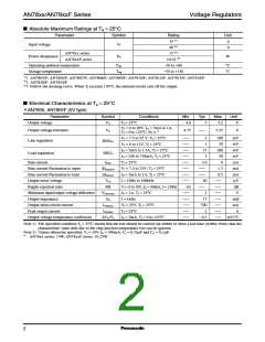
I Absolute Maximum Ratings at Ta = 25°C
Parameter
Symbol
Rating
Unit
V
1
*
*
*
35
40
15
Input voltage
VI
PD
2
3
V
AN78xx series
AN78xxF series
Power dissipation
W
3
*
10.25
Operating ambient temperature
Storage temperature
Topr
Tstg
−30 to +80
°C
°C
−55 to +150
*
*
*
1 AN7805/F, AN7806/F, AN7807/F, AN7808/F, AN7809/F, AN7810/F, AN7812/F, AN7815/F, AN7818/F
2 AN7820/F, AN7824/F
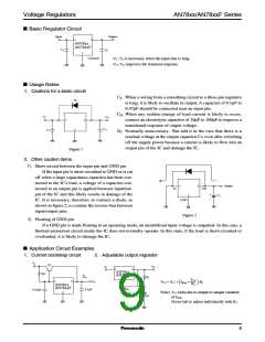
3 Follow the derating curve. When Tj exceeds 150°C, the internal circuit cuts off the output.
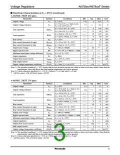
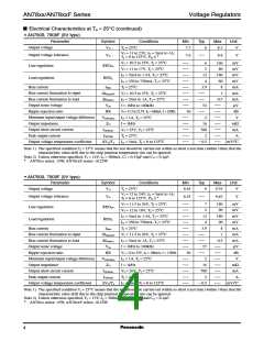
I Electrical Characteristics at Ta = 25°C
•
AN7805, AN7805F (5V type)
Parameter
Symbol
Conditions
Min
4.8
4.75
Typ
Max
5.2
Unit
Output voltage
Tj = 25°C
VI = 8 to 20V, IO = 5mA to 1A,
VO
5
V
Output voltage tolerance
Line regulation
VO
5.25
V
*
≤
Tj = 0 to 125°C, PD
VI = 7.5 to 25 V, Tj = 25°C
VI = 8 to 12V, Tj = 25°C
IO = 5mA to 1.5A, Tj = 25°C
IO = 250 to 750mA, Tj = 25°C
Tj = 25°C
3
1
100
50
mV
mV
mV
mV
mA
mA
mA
µV
REGIN
15
5
100
50
Load regulation
REGL
Bias current
IBias
∆IBias(IN)
∆IBias(L)
Vno
3.9
8
Bias current fluctuation to input
Bias current fluctuation to load
Output noise voltage
VI = 7.5 to 25V, Tj = 25°C
IO = 5mA to 1A, Tj = 25°C
f = 10Hz to 100kHz
1.3
0.5
40
Ripple rejection ratio
VI = 8 to 18V, IO = 100mA, f = 120Hz
RR
62
dB
Minimum input/output voltage difference
Output impedance
IO = 1A, Tj = 25°C
f = 1kHz
VDIF(min)
ZO
2
17
V
mΩ
mA
A
Output short-circuit current
Peak output current
VI = 25V, Tj = 25°C
Tj = 25°C
IO(Short)
IO(Peak)
∆VO/Ta
700
2
Output voltage temperature coefficient
IO = 5mA, Tj = 0 to 125°C
− 0.3
mV/°C
Note 1) The specified condition Tj = 25°C means that the test should be carried out within so short a test time (within 10ms) that the
characteristic value drift due to the chip junction temperature rise can be ignored.
Note 2) Unless otherwise specified, VI = 10V, IO = 500mA, CI = 0.33µF and CO = 0.1µF.
*
AN78xx series: 15W, AN78xxF series: 10.25W
2

 PANASONIC [ PANASONIC ]