PFS122
8bit MTP MCU with 12-bit R-Type ADC
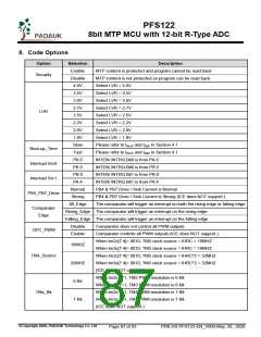
8. Code Options
Option
Selection
Enable
Disable
4.0V
Description
MTP content is protected and program cannot be read back
MTP content is not protected so program can be read back
Select LVR = 4.0V
Security
3.5V
Select LVR = 3.5V
3.0V
Select LVR = 3.0V
2.7V
Select LVR = 2.7V
LVR
2.5V
Select LVR = 2.5V
2.2V
Select LVR = 2.2V
2.0V
Select LVR = 2.0V
1.8V
Select LVR = 1.8V
Slow
Please refer to tWUP and tSBP in Section 4.1
Please refer to tWUP and tSBP in Section 4.1
INTEN/ INTRQ.Bit0 is from PA.0
INTEN/ INTRQ.Bit0 is from PB.5
INTEN/ INTRQ.Bit1 is from PB.0
INTEN/ INTRQ.Bit1 is from PA.4
PB4 & PB7 Drive / Sink Current is Normal
PB4 & PB7 Drive / Sink Current is Strong (ICE does NOT support.)
The comparator will trigger an interrupt on both the rising edge or falling edge
Boot-up_Time
Interrupt Src0
Interrupt Src1
PB4_PB7_Drive
Comparator
Fast
PA.0
PB.5
PB.0
PA.4
Normal
Strong
All_Edge
Rising_Edge The comparator will trigger an interrupt on the rising edge
Falling_Edge The comparator will trigger an interrupt on the falling edge
Edge
Disable
Enable
Comparator does not control all PWM outputs
Comparator controls all PWM outputs (ICE does NOT support.)
When tm2c[7:4]= 0010, TM2 clock source = IHRC = 16MHZ
When tm3c[7:4]= 0010, TM3 clock source = IHRC = 16MHZ
When tm2c[7:4]= 0010, TM2 clock source = IHRC*2 = 32MHZ
When tm3c[7:4]= 0010, TM3 clock source = IHRC*2 = 32MHZ
(ICE does NOT support.)
GPC_PWM
16MHZ
32MHZ
6 Bit
TMx_Source
When tm2s.7=1, TM2 PWM resolution is 6 Bit
When tm3s.7=1, TM3 PWM resolution is 6 Bit
When tm2s.7=1, TM2 PWM resolution is 7 Bit
When tm3s.7=1, TM3 PWM resolution is 7 Bit
(ICE does NOT support.)
TMx_Bit
7 Bit
©Copyright 2020, PADAUK Technology Co. Ltd
Page 87 of 93
PDK-DS-PFS122-EN_V000-May 28, 2020

 PADAUK [ PADAUK Technology ]