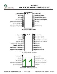
PFS122
8bit MTP MCU with 12-bit R-Type ADC
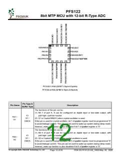
Pin Type &
Buffer Type
Pin Name
Description
The functions of this pin can be:
(1) Bit 3 of port B. It can be configured as digital input, two-state output with pull-high
/ pull-low resistor by software independently.
IO
PB3 /
AD3
ST /
(2) Channel 3 of ADC analog input
When this pin is configured as analog input, please use bit 3 of register pbdier to
disable the digital input to prevent current leakage. The bit 3 of pbdier register can
be set to “0” to disable digital input; wake-up from power-down by toggling this pin is
also disabled.
CMOS /
Analog
The functions of this pin can be:
(1) Bit 2 of port B. It can be configured as digital input, two-state output with pull-high
/ pull-low resistor by software independently.
IO
PB2 /
AD2 /
(2) Channel 2 of ADC analog input
ST /
(3) PWM output from Timer2
CMOS /
Analog
When this pin is configured as analog input, please use bit 2 of register pbdier to
disable the digital input to prevent current leakage. The bit 2 of pbdier register can
be set to “0” to disable digital input; wake-up from power-down by toggling this pin is
also disabled.
TM2PWM
The functions of this pin can be:
(1) Bit 1 of port B. It can be configured as digital input, two-state output with pull-high
/ pull-low resistor by software independently.
IO
PB1 /
AD1
ST /
(2) Channel 1 of ADC analog input
When this pin is configured as analog input, please use bit 1 of register pbdier to
disable the digital input to prevent current leakage. The bit 1 of pbdier register can
be set to “0” to disable digital input; wake-up from power-down by toggling this pin is
also disabled.
CMOS /
Analog
The functions of this pin can be:
(1) Bit 0 of port B. It can be configured as digital input, two-state output with pull-high
/ pull-low resistor by software independently.
(2) Channel 0 of ADC analog input
IO
PB0 /
AD0 /
INT1
(3) External interrupt line 1. It can be used as an external interrupt line 1. Both rising
edge and falling edge are accepted to request interrupt service and configurable
by register setting.
ST /
CMOS /
Analog
When this pin is configured as analog input, please use bit 0 of register pbdier to
disable the digital input to prevent current leakage. The bit 0 of pbdier register can be
set to “0” to disable digital input; wake-up from power-down by toggling this pin is also
disabled.
VDD: Digital positive power
VDD /
AVDD
VDD /
AVDD
AVDD: Analog positive power
VDD is the IC power supply while AVDD is the ADC power supply. AVDD and VDD
are double bonding internally and they have the same external pin.
GND: Digital negative power
GND /
AGND
GND /
AGND
AGND: Analog negative power
GND is the IC ground pin while AGND is the ADC ground pin. AGND and GND are
double bonding internally and they have the same external pin.
Notes: IO: Input/Output; ST: Schmitt Trigger input; Analog: Analog input pin; CMOS: CMOS voltage level
©Copyright 2020, PADAUK Technology Co. Ltd
Page 15 of 93
PDK-DS-PFS122-EN_V000-May 28, 2020

 PADAUK [ PADAUK Technology ]