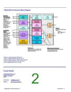
OXU210HP Architectural Block Diagram
SUPERIOR
PERFORMANCE
Large internal RAM
allows for multi-
buffering
72 KB
Buffer
Memory
OSC1
OSC2
PLL/
Clock
Test
Control
TEST
simultaneous
Transaction
Translator
streams. Retries due
to USB NAK’s are
done in hardware –
decreasing
interrupts and
lowering CPU and
bus utilization.
ACK
REQ
DMA
Interface
HS
OTG
Xcvr
Host
Controller
Power
2 PORTS
2 ports allow multiple usage
models;
Management
Transaction
Translator
LOW POWER
DESIGN
Multiple power and
clock regions are
available with
2 Hosts,
Host + Peripheral, or
Host + OTG
ADDR
DATA
CNTRL
INT
Host
Controller
16/32-bit
Microprocessor
Interface
HS
OTG
Xcvr
software-controlled
power saving
modes. PLL and
oscillator can be
disabled for deep-
sleep state. Clock
control block
produces the lowest
of four primary clock
frequencies that
meet the
Peripheral
Controller
System
Configuration &
Control Registers
OTG
Control
application’s
operational
requirements.
OTG LOGIC
Integrated hardware or software HNP
options allow for more control of your
software development.
SIMULTANEOUS OPERATION
Full host controller and peripheral controller
implementations allow both
to operate at the same time.
Windows is a registered trademark of Microsoft, Inc.
ThreadX is a registered trademark of Express Logic, Inc.
Nucleus is a registered trademark of Mentor Graphics Corporation.
VxWorks is a registered trademark of Wind River Systems.
Linux is a registered trademark of Linus Torvalds.
Contact Details
Oxford Semiconductor, Inc.
1768 McCandless Drive
Milpitas, CA. 95035
USA
Sales email:
sales@oxsemi.com
Website:
http://www.oxsemi.com
Copyright 2006, Oxford Semiconductor, Inc.
June 2006, REV. 1.1

 OXFORD [ OXFORD SEMICONDUCTOR ]