Page No. : 4/16
Detail Description
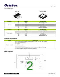
The RS7206 is a low‐dropout linear regulator. The device provides preset 2.5V, 2.85V and 3.3V output voltages for output
current up to 150mA. Other mask options for special output voltages from 1.2V to 5.0V with 100mV increment are also
available. As illustrated in function block diagram, it consists of a 1.0V reference, error amplifier, a P‐channel pass transistor,
an ON/OFF control logic and an internal feedback voltage divider.
The 1.0V band gap reference is connected to the error amplifier, which compares this reference with the feedback voltage
and amplifies the voltage difference. If the feedback voltage is lower than the reference voltage, the pass‐transistor gate is
pulled lower, which allows more current to pass to the output pin and increases the output voltage. If the feedback voltage is
too high, the pass transistor gate is pulled up to decrease the output voltage.
The output voltage is feed back through an internal resistive divider connected to VOUT pin. Additional blocks include an
output current limiter, thermal sensor, and shutdown logic.
Internal P‐channel Pass Transistor
The RS7206 features a P‐channel MOSFET pass transistor. Unlike similar designs using PNP pass transistors, P‐channel
MOSFETs require no base drive, which reduces quiescent current. PNP based regulators also waste considerable current in
dropout when the pass transistor saturates, and use high base‐drive currents under large loads. The RS7206 does not suffer
from these problems and consumes only 15μA (Typ.) of current consumption under heavy loads as well as in dropout
conditions.
Enable Function
EN pin starts and stops the regulator. When the EN pin is switched to the power off level, the operation of all internal circuit
stops, the build‐in P‐channel MOSFET output transistor between pins VIN and VOUT is switched off, allowing current
consumption to be drastically reduced. The VOUT pin enters the GND level through the internal discharge path between VOUT
and GND pins.
Output Voltage Selection
The RS7206 output voltage is preset at an internally trimmed voltage 2.5V, 2.85V or 3.3V. The output voltage also can be
mask‐optioned from 1.2V to 5.0V with 100mV increment by special order. The first two digits of part number suffix identify
the output voltage (see Ordering Information). For example, the RS7206‐33 has a preset 3.3V output voltage.
Current Limit
The RS7206 also includes a fold back current limiter. It monitors and controls the pass transistor’s gate voltage, estimates the
output current, and limits the output current within 0.5A.
Thermal Overload Protection
Thermal overload protection limits total power dissipation in the RS7206. When the junction temperature exceeds TJ=+150°C,
a thermal sensor turns off the pass transistor, allowing the IC to cool down. The thermal sensor turns the pass transistor on
again after the junction temperature cools down by 20°C, resulting in a pulsed output during continuous thermal overload
conditions.
Thermal overload protection is designed to protect the RS7206 in the event of fault conditions. For continuous operation, the
absolute maximum operating junction temperature rating of TJ=+125°C should not be exceeded.
Operating Region and Power Dissipation
Maximum power dissipation of the RS7206 depends on the thermal resistance of the case and circuit board, the temperature
difference between the die junction and ambient air, and the rate of airflow. The power dissipation across the devices is P =
IOUT x (VIN‐VOUT). The resulting maximum power dissipation is:
DS‐RS7206‐15 October, 2009
www.Orister.com

 ORISTER [ ORISTER CORPORATION ]