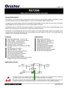
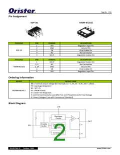
Page No. : 3/16
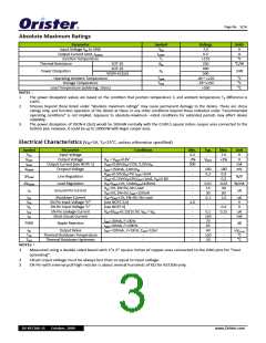
Absolute Maximum Ratings
Parameter
Input Voltage VIN to GND
Output Current Limit, I(LIMIT)
Junction Temperature
Symbol
VIN
ILIMIT
TJ
Ratings
7.0
0.5
+155
250
400
500
‐40 ~ +125
‐55~+150
+260
Units
V
A
oC
Thermal Resistance
SOT‐25
SOT‐25
VSON‐6 (2x2)
oC/W
θJA
Power Dissipation
PD
mW
Operating Ambient Temperature
Storage Temperature
Lead Temperature (soldering, 10sec)
TOPR
TSTG
‐
oC
oC
oC
NOTES:
1
The power dissipation values are based on the condition that junction temperature TJ and ambient temperature TA difference is
100°C.
2
Stresses beyond those listed under “absolute maximum ratings” may cause permanent damage to the device. These are stress
ratings only, and function operation of the device at these or any other conditions beyond those indicated under “recommended
operating conditions” is not implied. Exposure to absolute‐maximum –rated conditions for extended periods may affect device
reliability.
3
The power dissipation of VSON‐6 (2x2) would be 500mW normally with the 0.5X0.5 square inches cooper area connected to the
bottom pad. However, it could be up to 1000mW with larger cooper area.
Electrical Characteristics (VIN=5V, TA=25°C, unless otherwise specified)
Symbol
VIN
VOUT
IMAX
VDROP
Parameter
Input Voltage
Output Voltage
Conditions
Min.
2.2
‐2%
300
‐
‐
‐
‐
‐
Typ.
‐
VOUT
‐
160
0.2
‐
0.01
15
30
0.1
‐
Max.
7.0
+2%
‐
180
0.3
0.2
0.02
30
60
1.0
‐
0.3
0.15
‐
‐
‐
Unit
V
V
mA
mV
‐
VIN = VOUT+0.8V
Output Current (see NOTE 1)
Dropout Voltage
VOUT+0.8V≤VIN≤7.0V, 2.2V≤VIN
IOUT=150mA, 2.8V≤VIN
VOUT+0.5V≤VIN≤7V, IOUT=1mA
VOUT+0.15V≤VIN≤5V,IOUT=1mA, VIN≥2.8V
VIN=VOUT+1V, 1mA≤IOUT≤100mA
VIN=5V, EN=5V, No Load
VIN=5V, EN=5V, IOUT=150mA
VIN=VOUT+1V, EN=0V, No Load
(see NOTE 2,3)
ΔVLINE
ΔVLOAD
IQ
Line Regulation
Load Regulation
Ground Pin Current
%/V
%/mA
uA
‐
‐
ISD
VIH
VIL
IEN
ISC
Shutdown Current
EN Pin Input Voltage “H”
EN Pin Input Voltage “L”
EN Pin Leakage Current
Short Circuit Current
uA
V
V
uA
mA
2.0
‐
‐
‐
‐
‐
‐
‐
‐
(see NOTE 2)
‐
VIN=(VOUT+0.15) to 5V, VEN > VIH
‐
IOUT=30mA, F=1KHz
IOUT=30mA, F=10KHz
IOUT=100mA , F=1KHz, COUT=10uF
‐
0.1
150
70
65
40
150
20
PSRR
Ripple Rejection
dB
eN
TSD
THYS
Output Noise
Thermal Shutdown Temperature
Thermal Shutdown Hysteresis
‐
‐
‐
uV(rms)
oC
‐
oC
NOTES:
1
Measured using a double sided board with 1”x 2” square inches of copper area connected to the GND pins for “heat
spreading”.
2
3
EN pin input voltage must be always less than or equal to input voltage.
EN Pin with internal pull high resistor is about several hundreds of KΩ for RS7206 only.
DS‐RS7206‐15 October, 2009
www.Orister.com

 ORISTER [ ORISTER CORPORATION ]