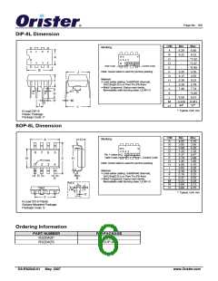
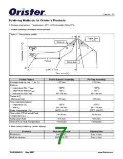
Page No. : 5/5
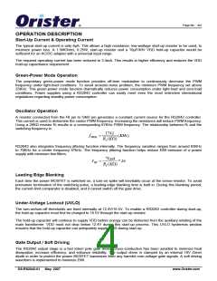
Slope Compensation
The sensed voltage across the current sense resistor is used for peak-current-mode control and cycle-by-cycle
current limiting. The built-in slope compensation function improves power supply stability and prevents peak-
current-mode control from causing sub-harmonic oscillations. Within every switching cycle, the RS2042 controller
produces a positively sloped, synchronized ramp signal.
Constant Output Power Limit
When the SENSE voltage across the sense resistor RS reaches the threshold voltage, the output GATE drive will
be turned off following a small propagation delay TPD. This propagation delay will result in an additional current
proportional to TPD*VIN/LP. The propagation delay is nearly constant regardless of the input line voltage VIN. Higher
input line voltages will result in larger additional currents. Thus, under high input-line voltages the output power limit
will be higher than under low input-line voltages.
The output power limit variation can be significant over a wide range of AC input voltages. To compensate for this,
the threshold voltage is adjusted by the current IIN. Since the pin VIN is connected to the rectified input line voltage
through the start-up resistor, a higher line voltage will result in a higher current IIN through the pin VIN.
The threshold voltage decreases if the current IIN increases. A small threshold voltage will force the output GATE
drive to terminate earlier, thus reducing total PWM turn-on time, and making the output power equal to that of the
low line input. This proprietary internal compensation feature ensures a constant output power limit over a wide
range of AC input voltages (90VAC to 264VAC).
VDD Over-voltage Protection
VDD over-voltage protection has been built in to prevent damage due to over voltage conditions. When the voltage
VDD exceeds the internal threshold due to abnormal conditions, PWM output will be turned off. Over-voltage
conditions are usually caused by open feedback loops.
Limited Power Control
The FB voltage will increase every time the output of the power supply is shorted or over-loaded. If the FB voltage
remains higher than a built-in threshold for longer than TLPS, PWM output will then be turned off. As PWM output is
turned off, the supply voltage VDD will also begin decreasing.
When VDD goes below the turn-off threshold (eg, 12.4V) the controller will be totally shut down. VDD will be
charged up to the turn-on threshold voltage of 16.5V through the start-up resistor until PWM output is restarted.
This protection feature will continue to be activated as long as the over-loading condition persists. This will prevent
the power supply from overheating due to over loading conditions.
Thermal Protection
An external NTC thermistor can be connected from the RT pin to ground. A fixed current IRT is sourced from the RT
pin. Because the impedance of the NTC will decrease at high temperatures, when the voltage of the RT pin drops
below 1.065V, PWM output will be disabled. The RT pin output current is related to the PWM frequency
programming resistor RI
Noise Immunity
Noise from the current sense or the control signal may cause significant pulse width jitter, particularly in continuous-
conduction mode. Slope compensation helps alleviate this problem. Good placement and layout practices should
be followed. The designer should avoiding long PCB traces and component leads. Compensation and filter
components should be located near the RS2042. Finally, increasing the power-MOS gate resistance is advised.
DS-RS2042-01 May, 2007
www.Orister.com

 ORISTER [ ORISTER CORPORATION ]