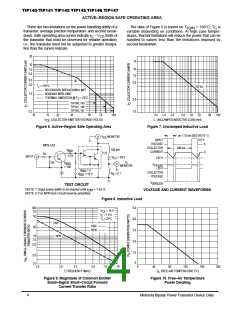
ACTIVE–REGION SAFE OPERATING AREA
There are two limitations on the power handling ability of a
transistor: average junction temperature and second break-
down. Safe operating area curves indicate I – V limits of
the transistor that must be observed for reliable operation;
i.e., the transistor must not be subjected to greater dissipa-
tion than the curves indicate.
The data of Figure 6 is based on T
= 150 C; T is
J(pk) C
variable depending on conditions. At high case temper-
atures, thermal limitations will reduce the power that can be
handled to values less than the limitations imposed by
second breakdown.
C
CE
20
15
10
10
7.0
5.0
7.0
3.0
2.0
dc
5.0
T
= 150°C
J
100 mJ
SECONDARY BREAKDOWN LIMIT
BONDING WIRE LIMIT
1.0
THERMAL LIMITATION @ T = 25°C
C
2.0
1.0
TIP140, 145
TIP141, 146
TIP142, 147
0.2
10
15
20
30
50
70
100
0.5
1.0
2.0
5.0
10
20
50
100
V
, COLLECTOR–EMITTER VOLTAGE (VOLTS)
L, UNCLAMPED INDUCTIVE LOAD (mH)
CE
Figure 6. Active–Region Safe Operating Area
Figure 7. Unclamped Inductive Load
w
≈
7.0 ms (SEE NOTE 1)
5.0 V
V
MONITOR
CE
INPUT
VOLTAGE
0
MPS–U52
COLLECTOR
CURRENT
100 ms
100 mH
R
BB1
0
TUT
50
1.5 k
INPUT
V
= 20 V
1.42 A
CC
I
50
C
R
= 100
BB2
V
CE(sat)
–20 V
MONITOR
V
= 0
= 10 V
BB2
COLLECTOR
VOLTAGE
R
= 0.1
V
S
BB1
V
(BR)CER
TEST CIRCUIT
NOTE 1: Input pulse width is increased until I
NOTE 2: For NPN test circuit reverse polarities.
= 1.42 A.
VOLTAGE AND CURRENT WAVEFORMS
CM
Figure 8. Inductive Load
100
70
5.0
V
= 10 V
CE
= 1.0 A
I
T
C
50
= 25°C
4.0
3.0
2.0
J
PNP
PNP
NPN
20
10
7.0
NPN
5.0
1.0
0
2.0
1.0
1.0
2.0
3.0
5.0
7.0
10
0
40
80
120
160
200
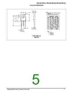
f, FREQUENCY (MHz)
T , FREE–AIR TEMPERATURE (°C)
A
Figure 9. Magnitude of Common Emitter
Small–Signal Short–Circuit Forward
Current Transfer Ratio
Figure 10. Free–Air Temperature
Power Derating
4
Motorola Bipolar Power Transistor Device Data

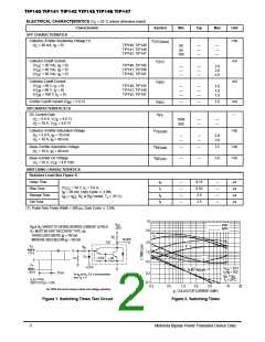
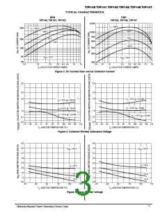
 ONSEMI [ ONSEMI ]