MOSFET - Power, Single
N-Channel
80 V, 29 mW, 22 A
NTMYS029N08LH
Features
www.onsemi.com
• Small Footprint (5x6 mm) for Compact Design
• Low R
to Minimize Conduction Losses
DS(on)
• Low Q and Capacitance to Minimize Driver Losses
G
V
R
MAX
I MAX
D
(BR)DSS
DS(ON)
• LFPAK4 Package, Industry Standard
29 mW @ 10 V
38 mW @ 4.5 V
• These Devices are Pb−Free and are RoHS Compliant
80 V
22 A
MAXIMUM RATINGS (T = 25°C unless otherwise noted)
J
Parameter
Drain−to−Source Voltage
Symbol
Value
80
20
22
15
33
17
7
Unit
V
D (5)
V
DSS
Gate−to−Source Voltage
V
GS
V
Continuous Drain
Current R
Steady
State
T
= 25°C
= 100°C
= 25°C
I
D
A
C
q
JC
G (4)
T
C
(Notes 1, 3)
Power Dissipation
T
C
P
D
W
A
S (1,2,3)
N−CHANNEL MOSFET
R
(Note 1)
q
JC
T
C
= 100°C
Continuous Drain
Current R
Steady
State
T = 25°C
A
I
D
q
JA
T = 100°C
A
5
(Notes 1, 2, 3)
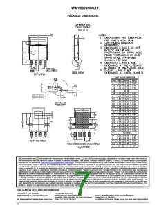
MARKING
DIAGRAM
Power Dissipation
T = 25°C
P
3.5
1.7
97
W
A
D
R
(Notes 1, 2)
q
JA
T = 100°C
A
D
Pulsed Drain Current
T = 25°C, t = 10 ms
I
DM
A
A
p
029N08
LH
AWLYW
Operating Junction and Storage Temperature
Range
T , T
−55 to
°C
J
stg
+175
LFPAK4
CASE 760AB
Source Current (Body Diode)
I
S
28
68
A
1
Single Pulse Drain−to−Source Avalanche
E
AS
mJ
S
S
S
G
Energy (I
= 1.0 A)
L(pk)
029N08LH = Specific Device Code
Lead Temperature for Soldering Purposes
T
260
°C
L
A
WL
Y
= Assembly Location
= Wafer Lot
= Year
(1/8″ from case for 10 s)
Stresses exceeding those listed in the Maximum Ratings table may damage the
device. If any of these limits are exceeded, device functionality should not be
assumed, damage may occur and reliability may be affected.
W
= Work Week
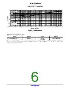
THERMAL RESISTANCE MAXIMUM RATINGS
ORDERING INFORMATION
See detailed ordering, marking and shipping information in the
package dimensions section on page 5 of this data sheet.
Parameter
Symbol
Value
4.6
Unit
Junction−to−Case − Steady State
Junction−to−Ambient − Steady State (Note 2)
R
°C/W
q
JC
R
42
q
JA
1. The entire application environment impacts the thermal resistance values shown,
they are not constants and are only valid for the particular conditions noted.
2
2. Surface−mounted on FR4 board using a 650 mm , 2 oz. Cu pad.
3. Maximum current for pulses as long as 1 second is higher but is dependent
on pulse duration and duty cycle.
© Semiconductor Components Industries, LLC, 2019
1
Publication Order Number:
February, 2020 − Rev. 0
NTMYS029N08LH/D

 ONSEMI [ ONSEMI ]