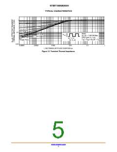
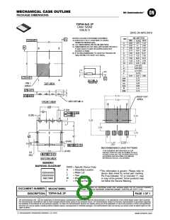
NTMT185N60S5H
THERMAL CHARACTERISTICS
Parameter
Symbol
Value
1.08
45
Unit
Thermal Resistance, Junction−to−Case, Max.
Thermal Resistance, Junction−to−Ambient, Max.
R
°C/W
q
JC
R
q
JA
ELECTRICAL CHARACTERISTICS (T = 25°C unless otherwise noted)
J
Parameter
Symbol
Test Conditions
Min
Typ
Max
Unit
OFF CHARACTERISTICS
Drain−to−Source Breakdown Voltage
V
V
I
= 0 V, I = 1 mA, T = 25_C
600
−
−
−
V
(BR)DSS
GS
D
J
Drain−to−Source Breakdown Voltage
Temperature Coefficient
DV
/
= 10 mA, Referenced to 25_C
−
630
mV/_C
(BR)DSS
D
DT
J
Zero Gate Voltage Drain Current
Gate−to−Source Leakage Current
ON CHARACTERISTICS
I
V
GS
= 0 V, V = 600 V, T = 25_C
−
−
−
−
2
mA
DSS
GSS
DS
J
I
V
=
30 V, V = 0 V
100
nA
GS
DS
Drain−to−Source On Resistance
Gate Threshold Voltage
R
V
= 10 V, I = 7.5 A, T = 25_C
−
2.7
−
148
−
185
4.3
−
mW
V
DS(on)
GS
D
J
V
V
GS
= V , I = 1.4 mA, T = 25_C
GS(th)
DS
D
J
Forward Trans−conductance
g
FS
V
DS
= 20 V, I = 7.5 A
18
S
D
CHARGES, CAPACITANCES & GATE RESISTANCE
Input Capacitance
C
V
= 400 V, V = 0 V, f = 250 kHz
−
−
−
1350
25
−
−
−
pF
ISS
DS
GS
Output Capacitance
C
OSS
Time Related Output Capacitance
C
I
= Constant, V = 0 V to 400 V,
372
OSS(tr.)
D
DS
= 0 V
V
GS
Energy Related Output Capacitance
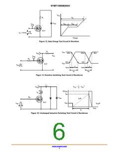
Total Gate Charge
C
V
= 0 V to 400 V, V = 0 V
−
−
−
−
−
42
25
7
−
−
−
−
−
OSS(er.)
DS
GS
Q
V
= 400 V, I = 7.5 A, V = 10 V
nC
G(tot)
DD
D
GS
Gate−to−Source Charge
Gate−to−Drain Charge
Gate Resistance
Q
GS
Q
8
GD
R
f = 1 MHz
0.9
W
G
SWITCHING CHARACTERISTICS
Turn-On Delay Time
Rise Time
t
V
GS
I
= 0/10 V, V = 400 V,
−
−
−
−
18
8
−
−
−
−
ns
d(on)
DD
= 7.5 A, R = 10 W
D
G
t
r
Turn-Off Delay Time
Fall Time
t
52
4.3
d(off)
t
f
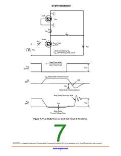
SOURCE-TO−DRAIN DIODE CHARACTERISTICS
Forward Diode Voltage
Reverse Recovery Time
Reverse Recovery Charge
V
V
GS
= 0 V, I = 7.5 A, T = 25_C
−
−
−
−
1.2
−
V
SD
RR
SD
J
t
V
= 0 V, I = 7.5 A,
213
2368
ns
nC
GS
SD
dI/dt = 100 A/ms, V = 400 V
DD
Q
−
RR
Product parametric performance is indicated in the Electrical Characteristics for the listed test conditions, unless otherwise noted. Product
performance may not be indicated by the Electrical Characteristics if operated under different conditions.
www.onsemi.com
2

 ONSEMI [ ONSEMI ]