NTBLS001N06C
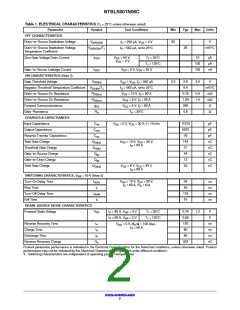
Table 1. ELECTRICAL CHARACTERISTICS (T = 25°C unless otherwise noted)
J
Parameter
OFF CHARACTERISTICS
Symbol
Test Conditions
Min
Typ
Max
Units
Drain−to−Source Breakdown Voltage
V
I
D
= 250 mA, V = 0 V
60
V
(BR)DSS
GS
Drain−to−Source Breakdown Voltage
Temperature Coefficient
V
/T
J
I = 562 mA, ref to 25°C
D
26
mV/°C
(BR)DSS
V
= 60 V,
GS
T = 25°C
10
Zero Gate Voltage Drain Current
I
mA
mA
nA
DS
J
DSS
V
= 0 V
T = 125°C
J
100
100
Gate−to−Source Leakage Current
ON CHARACTERISTICS (Note 3)
Gate Threshold Voltage
I
V
= 0 V, V = 20 V
GS
GSS
DS
GS
V
GS(th)
V
= V , I = 562 mA
2.0
2.8
9.9
4.0
V
mV/°C
mW
mW
S
DS
D
Negative Threshold Temperature Coefficient
Drain−to−Source On Resistance
Drain−to−Source On Resistance
Forward Transconductance
Gate−Resistance
V
/T
I = 562 mA, ref to 25°C
D
GS(th)
J
R
R
V
GS
= 10 V, I = 80 A
0.75
1.09
290
0.6
0.9
1.4
DS(on)
DS(on)
D
V
= 6 V, I = 56 A
D
GS
DS
g
V
= 5 V, I = 80 A
D
FS
R
T = 25°C
W
G
A
CHARGES & CAPACTIANCES
Input Capacitance
C
V
GS
= 0 V, V = 30 V, f = 10 kHz
11575
5973
76
pF
pF
pF
nC
nC
nC
nC
nC
iss
DS
Output Capacitance
C
oss
Reverse Transfer Capacitance
Total Gate Charge
C
rss
Q
V
GS
= 10 V, V = 30 V,
143
31
G(tot)
DS
I
= 80 A
D
Threshold Gate Charge
Q
G(th)
Gate−to−Source Charge
Gate−to−Drain Charge
Q
54
gs
gd
Q
13
Total Gate Charge
Q
V
GS
= 6 V, V = 30 V,
D
52
G(tot)
DS
I
= 80 A
SWITCHING CHARACTERISTICS, V = 10 V (Note 3)
GS
Turn−On Delay Time
Rise Time
t
V
= 10 V, V = 30 V,
34
53
ns
ns
ns
ns
d(on)
GS
D
DS
I
= 80 A, R = 6 W
G
t
r
Turn−Off Delay Time
Fall Time
t
119
91
d(off)
t
f
DRAIN−SOURCE DIODE CHARACTERISTICS
Forward Diode Voltage
V
I
I
= 80 A, V = 0 V
T = 25°C
0.79
0.66
120
60
1.2
V
V
SD
S
GS
J
= 80 A, V = 0 V
T = 125°C
J
S
GS
Reverse Recovery Time
Charge Time
t
ns
ns
ns
nC
V
GS
= 0 V, dI /d = 100 A/ms,
S t
rr
I
= 56 A
S
t
a
Discharge Time
t
60
b
Reverse Recovery Charge
Q
322
rr
Product parametric performance is indicated in the Electrical Characteristics for the listed test conditions, unless otherwise noted. Product
performance may not be indicated by the Electrical Characteristics if operated under different conditions.
3. Switching characteristics are independent of operating junction temperatures
www.onsemi.com
2

 ONSEMI [ ONSEMI ]