NL17SZ14
AC ELECTRICAL CHARACTERISTICS t = t = 3.0 ns
R
F
T
A
= 255C
*405C v T v 855C
A
V
(V)
CC
Min
Typ
Max
Min
Max
Symbol
Parameter
Condition
Unit
t
t
Propagation Delay
(Figure 3 and 4)
1.65
1.8
2.5 $ 0.2
3.3 $ 0.3
5.0 $ 0.5
2.0
2.0
1.0
1.0
0.5
9.1
7.6
5.0
3.7
3.1
15
12.5
9.0
6.3
5.2
2.0
2.0
1.0
1.0
0.5
15.6
13
9.5
6.5
5.5
ns
R = 1 MW, C = 15 pF
PLH
PHL
L
L
R = 500 W, C = 50 pF 3.3 $ 0.3
1.5
0.8
4.4
3.7
7.2
5.9
1.5
0.8
7.5
6.2
L
L
5.0 $ 0.5
CAPACITIVE CHARACTERISTICS
Symbol
Parameter
Condition
= 5.5 V, V = 0 V or V
Typical
Unit
pF
C
IN
Input Capacitance
V
u4.0
CC
I
CC
C
PD
Power Dissipation Capacitance
(Note 5)
10 MHz, V = 3.3 V, V = 0 V or V
25
30
pF
CC
I
CC
CC
10 MHz, V = 5.5 V, V = 0 V or V
CC
I
5. C is defined as the value of the internal equivalent capacitance which is calculated from the operating current consumption without load.
PD
Average operating current can be obtained by the equation: I
) = C ꢀ V ꢀ f + I . C is used to determine the no−load dynamic
CC(OPR
PD CC in CC PD
2
power consumption; P = C ꢀ V
ꢀ f + I ꢀ V
.
D
PD
CC
in
CC
CC
V
CC
A or B
OUTPUT
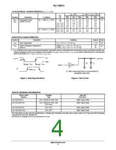
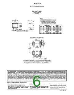
50%
GND
R
L
C
L
t
t
PLH
PHL
INPUT
Y
50% V
CC
A 1−MHz square input wave is recommended for
propagation delay tests.
Figure 3. Switching Waveform
Figure 4. Test Circuit
DEVICE ORDERING INFORMATION
Device Order
Number
Package
Type
Tape and
Reel Size
†
NL17SZ14DFT2
SOT−353/SC70−5/SC−88A
3000 / Tape & Reel
3000 / Tape & Reel
NL17SZ14DFT2G
SOT−353/SC70−5/SC−88A
(Pb−Free)
NL17SZ14XV5T2
NL17SZ14XV5T2G
SOT−553*
SOT−553*
3000 / Tape & Reel
3000 / Tape & Reel
†For information on tape and reel specifications, including part orientation and tape sizes, please refer to our Tape and Reel Packaging
Specifications Brochure, BRD8011/D.
*All Devices in Package SOT553 are Inherently Pb−Free.
http://onsemi.com
4

 ONSEMI [ ONSEMI ]