NL17SZ14
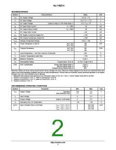
MAXIMUM RATINGS
Symbol
Characteristics
Value
Unit
V
V
DC Supply Voltage
*0.5 to )7.0
CC
V
DC Input Voltage
*0.5 ≤ V ≤ )7.0
V
I
O
I
V
DC Output Voltage
Output in High or LOW State (Note 1)
V < GND
*0.5 ≤ V ≤ 7.0
V
O
I
DC Input Diode Current
DC Output Diode Current
DC Output Sink Current
DC Supply Current per Supply Pin
DC Ground Current per Ground Pin
Storage Temperature Range
Power Dissipation in Still Air
*50
*50
mA
mA
mA
mA
mA
°C
IK
I
I
V < GND
O
OK
I
$50
O
I
$100
CC
I
$100
GND
T
*65 to )150
STG
P
SOT−353
SOT−553
186
135
mW
D
q
Thermal Resistance
SOT−353
SOT−553
350
496
°C/W
JA
T
Lead Temperature, 1 mm from Case for 10 Seconds
Junction Temperature under Bias
Moisture Sensitivity
260
)150
°C
°C
L
J
T
MSL
Level 1
F
Flammability Rating
Oxygen Index: 28 to 34
UL 94 V−0 @ 0.125 in
R
ESD
ESD Classification
Human Body Model (Note 2)
Machine Model (Note 3)
Charged Device Model (Note 4)
Class 2
Class C
N/A
Maximum ratings are those values beyond which device damage can occur. Maximum ratings applied to the device are individual stress limit
values (not normal operating conditions) and are not valid simultaneously. If these limits are exceeded, device functional operation is not implied,
damage may occur and reliability may be affected.
1. Measured with minimum pad spacing on an FR4 board, using 10 mm−by−1 inch, 2−ounce copper trace with no air flow.
2. Tested to EIA/JESD22−A114−A, rated to EIA/JESD22−A114−B.
3. Tested to EIA/JESD22−A115−A, rated to EIA/JESD22−A115−A.
4. Tested to JESD22−C101−A.
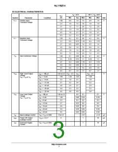
RECOMMENDED OPERATING CONDITIONS
Symbol
Parameter
Min
Max
Unit
V
Supply Voltage
Operating
Data Retention Only
1.65
1.5
5.5
5.5
V
CC
V
Input Voltage
0
0
5.5
5.5
V
V
I
V
Output Voltage
(High or LOW State)
O
T
Operating Free−Air Temperature
Input Transition Rise or Fall Rate
*40
)85
°C
A
Dt/DV
V
V
V
= 2.5 V $0.2 V
= 3.0 V $0.3 V
= 5.0 V $0.5 V
0
0
0
No Limit
No Limit
No Limit
ns/V
CC
CC
CC
http://onsemi.com
2

 ONSEMI [ ONSEMI ]