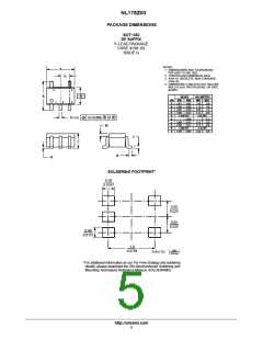
NL17SZ00
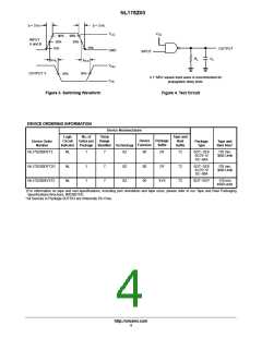
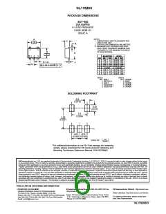
t = 3 ns
f
t = 3 ns
f
V
CC
V
CC
90%
50%
90%
50%
INPUT
A and B
10%
10%
OUTPUT
GND
INPUT
R
C
L
L
t
t
PHL
PLH
V
V
OH
OUTPUT Y
50%
50%
A 1−MHz square input wave is recommended for
propagation delay tests.
OL
Figure 3. Switching Waveform
Figure 4. Test Circuit
DEVICE ORDERING INFORMATION
Device Nomenclature
Temp
Logic
No. of
Tape and
Device
Function
Package
Suffix
Circuit
Gates per
Range
Reel
Suffix
Device Order
Number
Package
Type
Tape and
Reel Size
†
Indicator Package Identifier
Technology
NL17SZ00DFT2
NL17SZ00DFT2G
NL17SZ00XV5T2
NL
NL
NL
1
1
1
7
7
7
SZ
00
00
00
DF
T2
T2
T2
SOT−353/
SC70−5/
SC−88A
178 mm,
3000 Units
SZ
SZ
DF
SOT−353/
SC70−5/
SC−88A
178 mm,
3000 Units
XV5
SOT−553*
178 mm
4000 units
†For information on tape and reel specifications, including part orientation and tape sizes, please refer to our Tape and Reel Packaging
Specifications Brochure, BRD8011/D.
*All Devices in Package SOT553 are Inherently Pb−Free.
http://onsemi.com
4

 ONSEMI [ ONSEMI ]