NDC7002N
TYPICAL THERMAL CHARACTERISTICS
0.55
1.2
1.1
1
1a
0.5
1a
1b
1c
1b
0.45
1c
0.9
0.8
0.7
0.6
4.5″ x 5″ FR−4 Board
0.4
4.5″ x 5″ FR−4 Board
T = 25°C’
A
T = 25°C
A
Still Air
Still Air
V
GS
= 10 V
0.35
0
0.2
0.4
0.6
0.8
1
0
0.025
0.05
0.075
0.1
0.125
2
2
2oz Copper Mounting Pad Area (in )
2oz Copper Mounting Pad Area (in )
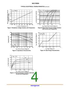
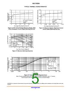
Figure 12. SOT−6 Dual Package Maximum Steady−State
Figure 13. Maximum Steady−State Drain Current
Power Dissipation versus Copper Mounting Pad Area
versus Copper Mounting Pad Area
3
2
1
0.5
0.2
0.1
V
= 10 V
GS
0.05
Single Pulse
R
= See Note 1c
q
JA
0.02
0.01
T = 25°C
A
1
2
5
10
20
50 70
V
DS
, Drain−Source Voltage (V)
Figure 14. Maximum Safe Operating Area
1
D = 0.5
0.5
0.2
R
R
(t) = r(t) * R
q
JA
= See Note 1c
q
q
JA
JA
0.2
0.1
0.1
P(pk)
0.05
0.02
0.01
Single Pulse
t
0.05
1
t
2
T − T = P * R (t)
Duty Cycle, D = t /t
q
JA
1
J
A
0.02
0.01
2
0.001
0.1
t , Time (sec)
1
10
100
300
0.0001
0.01
1
Figure 15. Transient Thermal Response Curve
(Note: Thermal characterization performed using the conditions described in note 1c. Transient
thermal response will change depending on the circuit board design.)
SUPERSOT is a trademark of Semiconductor Components Industries, LLC dba “onsemi” or its affiliates and/or subsidiaries in the United States and/or other
countries.
www.onsemi.com
5

 ONSEMI [ ONSEMI ]