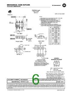
NDC7002N
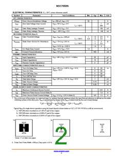
ELECTRICAL CHARACTERISTICS (TA = 25°C unless otherwise noted)
Symbol
Parameter
Test Conditions
Min
Typ
Max
Unit
OFF CHARACTERISTICS
BV
Drain−Source Breakdown Voltage
I
D
= 250 mA, V = 0 V
50
V
DSS
GS
I
Zero Gate Voltage Drain Current
V
DS
= 40 V, V = 0 V
1
500
mA
DSS
GS
T = 125°C
J
I
Gate−Body Leakage, Forward
Gate−Body Leakage, Reverse
V
V
= 20 V, V = 0 V
100
nA
nA
GSSF
GS
DS
I
= −20 V, V = 0 V
−100
GSSR
GS
DS
ON CHARACTERISTICS (Note 2)
V
Gate Threshold Voltage
V
V
= V , I = 250 mA
1
0.8
1.9
1.5
2.5
2.2
V
GS(th)
GS
DS
D
T = 125°C
J
R
Static Drain−Source On−Resistance
= 10 V, I = 0.51 A
1
1.7
2
3.5
W
DS(ON)
GS
D
T = 125°C
J
V
GS
V
GS
V
DS
= 4.5 V, I = 0.35 A
1.6
4
D
I
On−State Drain Current
= 10 V, V = 10 V
1.5
A
D(on)
DS
g
FS
Forward Transconductance
= 10 V, I = 0.51 A
400
mS
D
DYNAMIC CHARACTERISTICS
C
Input Capacitance
V
DS
= 25 V, V = 0 V, f = 1.0 MHz
20
13
5
pF
pF
pF
iss
GS
C
Output Capacitance
oss
C
Reverse Transfer Capacitance
rss
SWITCHING CHARACTERISTICS (Note 2)
t
Turn−On Delay Time
Turn−On Time
V
= 25 V, I = 0.25 A, V = 10 V,
GEN
6
6
20
20
20
20
ns
d(on)
DD
D
GS
R
= 25 W
t
r
t
Turn−Off Delay Time
Turn−Off Fall Time
Total Gate Charge
Gate−Source Charge
Gate to Drain Charge
11
5
d(off)
t
f
Q
V
DS
= 25 V, I = 0.51 A, V = 10 V
1
nC
nC
nC
g
D
GS
Q
0.19
0.33
gs
gd
Q
DRAIN−SOURCE DIODE CHARACTERISTICS
I
Maximum Continuous Source Current
Maximum Pulse Source Current (Note 2)
Drain−Source Diode Forward Voltage
0.51
1.5
A
A
V
S
I
SM
V
SD
V
GS
= 0 V, I = 0.51 A (Note 2)
0.8
1.2
S
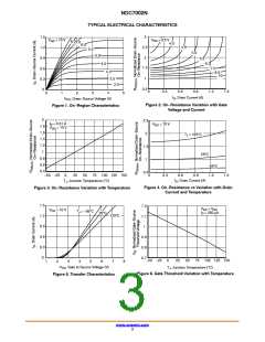
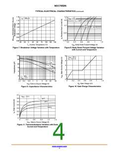
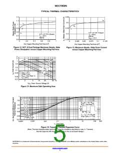
1. R
is the sum of the junction−to−case and case−to−ambient thermal resistance where the case thermal reference is defined as the solder
θ
JA
mounting surface of the drain pins. R
is guaranteed by design while R
is determined by the user’s board design.
θ
θ
JC
CA
TJ * TA
TJ * TA
qJC ) RqCA(t)
PD(t) +
+
+ I2D(t) RDS(ON)@TJ
R
qJA(t)
R
Typical R
for single device operation using the board layouts shown below on 4.5″ x 5″ FR−4 PCB in a still air environment:
q
JA
2
a. 130°C/W when mounted on a 0.125 in pad of 2oz copper.
b. 140°C/W when mounted on a 0.005 in pad of 2oz copper.
c. 180°C/W when mounted on a 0.0015 in pad of 2oz copper.
2
2
1a
1b
1c
Scale 1:1 on letter size paper
2. Pulse Test: Pulse Width ≤ 300 ms, Duty cycle ≤ 2.0 %.
www.onsemi.com
2

 ONSEMI [ ONSEMI ]