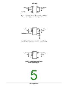
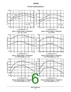
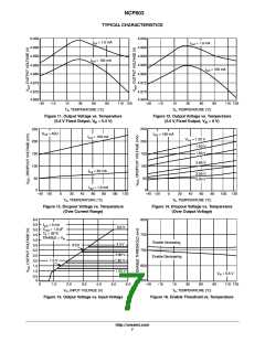
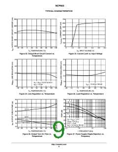
NCP603
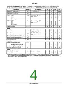
ELECTRICAL CHARACTERISTICS (V = 1.750 V, V = 1.250 V (adjustable version)), (V = V + 0.5 V (fixed version)),
in
out
in
out
C
= C =1.0 mF, for typical values T = 25°C, for min/max values T = -40°C to 125°C, unless otherwise specified.) (Note 10)
out A A
in
Characteristic
Symbol
Test Conditions
f = 10 Hz to 100 kHz
Min
Typ
Max
Unit
Output Noise Voltage (Note 11)
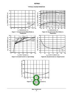
Output Short Circuit Current
-
50
-
mV
rms
V
n
500
650
900
mA
mV
I
sc
Dropout Voltage
1.3 V
1.5 V
V
Measured at: V – 2.0%
out
DO
DO
-
-
-
-
175
150
125
75
250
225
175
125
I
= 150 mA
out
1.8 V
2.7 V to 5.0 V
Dropout Voltage
1.3 V
1.5 V
V
mV
mA
Measured at: V
out
– 2.0%
-
-
-
-
375
350
245
157
480
400
340
230
I
= 300 mA
out
1.8 V
2.7 V to 5.0 V
Output Current Limit
300
650
-
I
out(max)
General
Disable Current
I
ENABLE = 0 V, Vin = 6 V
-
-
0.01
145
1.0
mA
mA
DIS
-40°C ≤ T ≤ 85°C
A
Ground Current
I
ENABLE = 0.9 V,
180
GND
I
= 1.0 mA to 300 mA
out
Thermal Shutdown Temperature (Note 11)
Thermal Shutdown Hysteresis (Note 11)
ADJ Input Bias Current
T
-
-
175
10
-
-
-
°C
°C
mA
SD
T
SH
I
-0.75
0.75
ADJ
Chip Enable
ENABLE Input Threshold Voltage
V
th(EN)
V
Voltage Increasing, Logic High
Voltage Decreasing, Logic Low
Enable Input Bias Current (Note 11)
Timing
0.9
-
-
-
-
0.4
100
I
t
-
3.0
nA
EN
Output Turn On Time (Note 11)
1.25 V to 3.5 V
5.0 V
ms
ENABLE = 0 V to V
in
EN
-
-
15
30
25
50
10.Performance guaranteed over the indicated operating temperature range by design and/or characterization, production tested at T = T =
A
J
25°C. Low duty cycle pulse techniques are used during testing to maintain the junction temperature as close to ambient as possible.
11. Values based on design and/or characterization.
http://onsemi.com
4

 ONSEMI [ ONSEMI ]