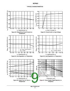
NCP603
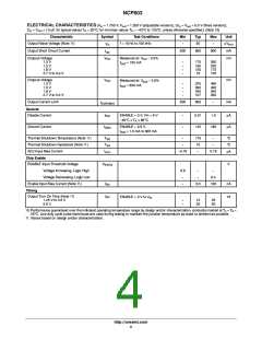
ELECTRICAL CHARACTERISTICS (V = 1.750 V, V = 1.250 V, C = C =1.0 mF, for typical values T = 25°C, for min/max
in
out
in
out
A
values T = -40°C to 125°C, unless otherwise specified.) (Note 8)
A
Characteristic
Symbol
Test Conditions
Min
Typ
Max
Unit
Regulator Output (Adjustable Voltage Version)
Output Voltage
Output Voltage
V
I
V
V
= 1.0 mA to 150 mA
= 1.75 V to 6.0 V,
= ADJ
1.231
(-1.5%)
1.250
1.269
(+1.5%)
V
out
out
in
out
1.213
(-3%)
1.250
1.287
(+3%)
V
V
I
= 1.0 mA to 300 mA
out
out
V
V
= 1.75 V to 6.0 V,
= ADJ = 1.25 V
in
out
Power Supply Ripple Rejection (Note 9)
PSRR
dB
I
= 1.0 mA to 150 mA
out
V
= V + 1 V + 0.5 V
p-p
out
in
-
-
-
62
55
38
-
-
-
f = 120 Hz
f = 1.0 kHz
f = 10 kHz
Line Regulation
-
1.0
10
mV
mV
Reg
line
V
I
= 1.750 V to 6.0 V,
= 1.0 mA
in
out
Load Regulation
-
-
2.0
50
45
-
Reg
load
I
= 1.0 mA to 300 mA
out
Output Noise Voltage (Note 9)
Output Short Circuit Current
f = 10 Hz to 100 kHz
mV
rms
V
n
500
650
900
mA
mV
I
sc
Dropout Voltage
1.25 V
V
DO
Measured at: V
– 2.0%,
= 150 mA, Figure 2
out
-
175
250
I
out
Dropout Voltage
1.25 V
V
mV
mA
Measured at: V
– 2.0%,
= 300 mA, Figure 2
DO
out
-
375
650
480
-
I
out
Output Current Limit
300
I
out(max)
Regulator Output (Fixed Voltage Version) (V = V + 0.5 V, C = C =1.0 mF, for typical values T = 25°C, for min/max values T =
in
out
in
out
A
A
-40°C to 125°C; unless otherwise noted.) (Note 8)
Output Voltage
1.3 V
1.5 V
(-2%)
1.270
1.470
1.764
2.744
2.940
3.234
3.43
(+2%)
1.326
1.530
1.836
2.856
3.060
3.366
3.57
V
V
I
= 1.0 mA to 150 mA
out
out
V
1.3
1.5
1.8
2.8
3.0
3.3
3.5
5.0
= (V + 0.5 V) to 6.0 V
in
out
1.8 V
2.8 V
3.0 V
3.3 V
3.5 V
5.0 V
4.900
5.100
Output Voltage
1.3 V
1.5 V
(-3%)
1.261
1.455
1.746
2.716
2.910
3.201
3.395
4.850
(+3%)
1.339
1.545
1.854
2.884
3.090
3.399
3.605
5.150
V
V
I
out
= 1.0 mA to 300 mA
out
1.3
1.5
1.8
2.8
3.0
3.3
3.5
5.0
V
in
= (V + 0.5 V) to 6.0 V
out
1.8 V
2.8 V
3.0 V
3.3 V
3.5 V
5.0 V
Power Supply Ripple Rejection (Note 9)
PSRR
dB
I
= 1.0 mA to 150 mA
out
V
= V + 1 V + 0.5 V
p-p
out
in
-
-
-
62
55
38
-
-
-
f = 120 Hz
f = 1.0 kHz
f = 10 kHz
Line Regulation
Load Regulation
-
1.0
10
mV
mV
Reg
line
V
I
= 1.750 V to 6.0 V,
= 1.0 mA
in
out
-
-
2.0
2.0
30
45
Reg
load
I
I
= 1.0 mA to 150 mA
= 1.0 mA to 300 mA
out
out
8. Performance guaranteed over the indicated operating temperature range by design and/or characterization, production tested at T = T =
A
J
25°C. Low duty cycle pulse techniques are used during testing to maintain the junction temperature as close to ambient as possible.
9. Values based on design and/or characterization.
http://onsemi.com
3

 ONSEMI [ ONSEMI ]