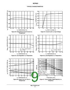
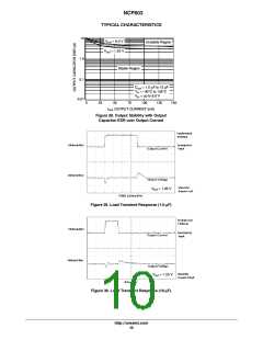
NCP603
Noise Decoupling
Thermal
The NCP603 is a low noise regulator and needs no
external noise reduction capacitor. Unlike other low noise
regulators which require an external capacitor and have slow
startup times, the NCP603 operates without a noise
reduction capacitor, has a typical 15 ms start up delay and
As power in the NCP603 increases, it might become
necessary to provide some thermal relief. The maximum
power dissipation supported by the device is dependent
upon board design and layout. Mounting pad configuration
on the PCB, the board material, and the ambient temperature
affect the rate of junction temperature rise for the part. When
the NCP603 has good thermal conductivity through the
PCB, the junction temperature will be relatively low with
high power applications. The maximum dissipation the
NCP603 can handle is given by:
achieves a 50 mV overall noise level between 10 Hz and
rms
100 kHz.
Enable Operation
The enable pin will turn the regulator on or off. The
threshold limits are covered in the electrical characteristics
table in this data sheet. The turn-on/turn-off transient
voltage being supplied to the enable pin should exceed a
slew rate of 10 mV/ms to ensure correct operation. If the
enable function is not to be used then the pin should be
T
* T
A
J(MAX)
P
+
D(MAX)
(eq. 3)
R
qJA
Since T is not recommended to exceed 125_C (T
),
then the NCP603 can dissipate up to 465 mW when the
J
J(MAX)
ambient temperature (T ) is 25_C and the device is
A
assembled on 1 oz PCB with 645 mm area.
connected to V .
in
2
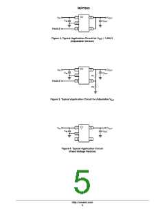
Output Voltage Adjust
The power dissipated by the NCP603 can be calculated
from the following equations:
The output voltage can be adjusted from 1 times
(Figureꢁ2) to 4 times (Figure 3) the typical 1.250 V
regulation voltage via the use of resistors between the output
and the ADJ input. The output voltage and resistors are
chosen using Equation 1 and Equation 2.
P
D
[ V (I
) ) I (V * V )
OUT IN OUT
IN GND@IOUT
(eq. 4)
(eq. 5)
or
P
) (V
OUT
I
)
OUT
D(MAX)
R1
+ 1.250ꢀǒ1 ) Ǔ) (I
V
[
IN(MAX)
V
OUT
R1)
(eq. 1)
I
) I
GND
ADJ
OUT
R2
[V
(I
* R1)]
out * ADJ
1.25
V
out
1.25
ƪ
* 1ƫ
(eq. 2)
R1 + R2 * ƪ
* 1ƫ^ R2ꢀ
Hints
V and GND printed circuit board traces should be as
in
wide as possible. When the impedance of these traces is
high, there is a chance to pick up noise or cause the regulator
to malfunction. Place external components, especially the
output capacitor, as close as possible to the NCP603, and
make traces as short as possible.
Input bias current I
is typically less than 150 nA.
ADJ
Choose R2 arbitrarily t minimize errors due to the bias
current and to minimize noise contribution to the output
voltage. Use Equation 2 to find the required value for R1.
DEVICE ORDERING INFORMATION
Device
NCP603SNADJT1G
Marking Code
AAU
Version
ADJ
Package
Shipping*
NCP603SN130T1G
NCP603SN150T1G
NCP603SN180T1G
NCP603SN280T1G
NCP603SN300T1G
NCP603SN330T1G
NCP603SN350T1G
NCP603SN500T1G
AAF
1.3 V
1.5 V
1.8 V
2.8 V
3.0 V
3.3 V
3.5 V
5.0 V
AAV
AAW
AAX
TSOP-5
(Pb-Free)
3000/Tape & Reel
AAY
AAZ
AA2
AA3
*For additional information on our Pb-Free strategy and soldering details, please download the ON Semiconductor Soldering and Mounting
Techniques Reference Manual, SOLDERRM/D.
http://onsemi.com
12

 ONSEMI [ ONSEMI ]