NCP603
DEFINITIONS
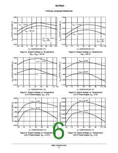
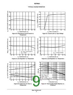
Load Regulation
Line Regulation
The change in output voltage for a change in output load
current at a constant temperature.
The change in output voltage for a change in input voltage.
The measurement is made under conditions of low
dissipation or by using pulse techniques such that the
average junction temperature is not significantly affected.
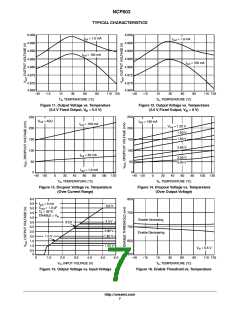
Dropout Voltage
The input/output differential at which the regulator output
no longer maintains regulation against further reductions in
input voltage. Measured when the output drops 2% below its
nominal. The junction temperature, load current, and
minimum input supply requirements affect the dropout level.
Line Transient Response
Typical output voltage overshoot and undershoot
response when the input voltage is excited with a given
slope.
Output Noise Voltage
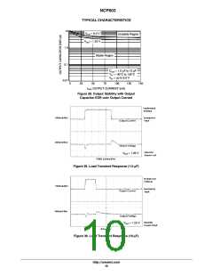
Load Transient Response
This is the integrated value of the output noise over a
specified frequency range. Input voltage and output load
current are kept constant during the measurement. Results
Typical output voltage overshoot and undershoot
response when the output current is excited with a given
slope between no-load and full-load conditions.
are expressed in mV or nV √ Hz.
rms
Thermal Protection
Internal thermal shutdown circuitry is provided to protect
the integrated circuit in the event that the maximum junction
temperature is exceeded. When activated at typically 175°C,
the regulator turns off. This feature is provided to prevent
failures from accidental overheating.
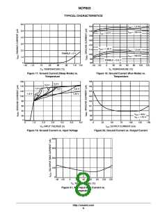
Ground Current
Ground Current is the current that flows through the
ground pin when the regulator operates without a load on its
output (I
). This consists of internal IC operation, bias,
GND
etc. It is actually the difference between the input current
(measured through the LDO input pin) and the output load
current. If the regulator has an input pin that reduces its
internal bias and shuts off the output (enable/disable
Maximum Package Power Dissipation
The power dissipation level at which the junction
temperature reaches its maximum operating value.
function), this term is called the standby current (I
.)
STBY
APPLICATIONS INFORMATION
The NCP603 series regulator is self-protected with
output, there is no resistor divider. If the part is enabled
under no-load conditions, leakage current through the pass
transistor at junction temperatures above 85°C can approach
several microamperes, especially as junction temperature
approaches 150°C. If this leakage current is not directed into
a load, the output voltage will rise up to a level
approximately 20 mV above nominal.
The NCP603 contains an overshoot clamp circuit to
improve transient response during a load current step
release. When output voltage exceeds the nominal by
approximately 20 mV, this circuit becomes active and
clamps the output from further voltage increase. Tying the
internal thermal shutdown and internal current limit. Typical
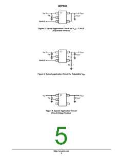
application circuits are shown in Figures 2 and 3.
Input Decoupling (Cin)
A ceramic or tantalum 1.0 mF capacitor is recommended
and should be connected close to the NCP603 package.
Higher capacitance and lower ESR will improve the overall
line transient response.
Output Decoupling (Cout
)
The NCP603 is a stable component and does not require
a minimum Equivalent Series Resistance (ESR) for the
output capacitor. The minimum output decoupling value is
1.0 mF and can be augmented to fulfill stringent load
transient requirements. The regulator works with ceramic
chip capacitors as well as tantalum devices. Larger values
improve noise rejection and load regulation transient
response. Figure 28 shows the stability region for a range of
operating conditions and ESR values.
ENABLE pin to V will ensure that the part is active
in
whenever the supply voltage is present, thus guaranteeing
that the clamp circuit is active whenever leakage current is
present.
When the NCP603 adjustable regulator is disabled, the
overshoot clamp circuit becomes inactive and the pass
transistor leakage will charge any capacitance on V . If no
out
load is present, the output can charge up to within a few
millivolts of V . In most applications, the load will present
No-Load Regulation Considerations
in
some impedance to V such that the output voltage will be
The NCP603 adjustable regulator will operate properly
under conditions where the only load current is through the
resistor divider that sets the output voltage. However, in the
case where the NCP603 is configured to provide a 1.250 V
out
inherently clamped at a safe level. A minimum load of
10ꢁmA is recommended.
http://onsemi.com
11

 ONSEMI [ ONSEMI ]