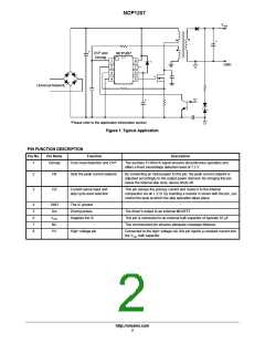
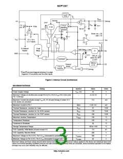
NCP1207
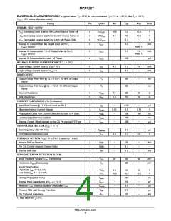
ELECTRICAL CHARACTERISTICS (For typical values T = 25°C, for min/max values T = 0°C to +125°C, Max T = 150°C,
J
J
J
V
CC
= 11 V unless otherwise noted)
Rating
Pin
Symbol
Min
Typ
Max
Unit
DYNAMIC SELF−SUPPLY
V
V
V
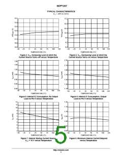
Increasing Level at which the Current Source Turns−off
6
6
6
6
VCC
10.8
9.1
−
12
10
12.9
10.6
−
V
V
CC
CC
CC
OFF
Decreasing Level at which the Current Source Turns−on
Decreasing Level at which the Latch−off Phase Ends
VCC
ON
VCC
5.3
1.0
V
latch
Internal IC Consumption, No Output Load on Pin 5,
= 60 kHz
I
I
I
−
1.3
(Note 1)
mA
CC1
F
SW
Internal IC Consumption, 1.0 nF Output Load on Pin 5,
= 60 kHz
6
6
−
−
1.6
2.0
(Note 1)
mA
CC2
CC3
F
SW
Internal IC Consumption in Latch−off Phase
330
−
mA
INTERNAL STARTUP CURRENT SOURCE (T u 0°C)
J
High−voltage Current Source, V = 10 V
8
8
I
I
4.3
−
7.0
8.0
9.6
−
mA
mA
CC
C1
High−voltage Current Source, V = 0
CC
C2
DRIVE OUTPUT
Output Voltage Rise−time @ CL = 1.0 nF, 10−90% of Output
Signal
5
5
T
−
−
40
20
−
−
ns
ns
r
Output Voltage Fall−time @ CL = 1.0 nF, 10−90% of Output
Signal
T
f
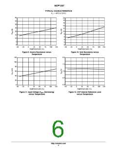
Source Resistance
5
5
R
12
20
10
36
19
W
W
OH
Sink Resistance
R
5.0
OL
CURRENT COMPARATOR (Pin 5 Unloaded)
Input Bias Current @ 1.0 V Input Level on Pin 3
Maximum Internal Current Setpoint
3
3
3
3
3
I
−
0.92
−
0.02
1.0
−
1.12
160
−
mA
V
IB
I
Limit
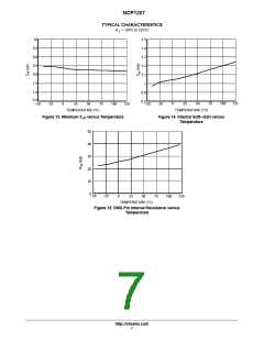
Propagation Delay from Current Detection to Gate OFF State
Leading Edge Blanking Duration
T
DEL
T
LEB
skip
100
380
200
ns
ns
mA
−
Internal Current Offset Injected on the CS Pin during OFF Time
I
−
−
OVERVOLTAGE SECTION (V = 11 V)
CC
Sampling Delay after ON Time
OVP Internal Reference Level
1
1
T
−
4.5
7.2
−
ms
sample
V
ref
6.4
8.0
V
FEEDBACK SECTION (V = 11 V, Pin 5 Loaded by 1.0 kW)
CC
Internal Pull−up Resistor
2
−
−
Rup
Iratio
Tss
−
−
−
20
3.3
1.0
−
−
−
kW
−
Pin 3 to Current Setpoint Division Ratio
Internal Soft−start
ms
DEMAGNETIZATION DETECTION BLOCK
Input Threshold Voltage (V
Decreasing)
1
1
V
35
−
50
20
90
−
mV
mV
pin1
TH
Hysteresis (V
Decreasing)
V
H
pin1
Input Clamp Voltage
High State (I 1 = 3.0 mA)
1
1
VC
8.0
10
12
V
V
pin
H
Low State (I 1 = −2.0 mA)
pin
VC
−0.9
−0.7
−0.5
L
Demag Propagation Delay
1
1
1
1
1
T
−
−
−
−
−
210
10
−
−
−
−
−
ns
pF
ms
dem
Internal Input Capacitance at V
= 1.0 V
C
par
pin1
Minimum T
(Internal Blanking Delay after T
)
T
blank
8.0
5.0
28
OFF
ON
Timeout After Last Demag Transition
Pin 1 Internal Impedance
T
ms
out
R
kW
int
1. Max value at T = 0°C.
J
http://onsemi.com
4

 ONSEMI [ ONSEMI ]