NCP1200
V
CC
Regulation
Occurs Here
11.4 V
Latchoff
Phase
9.8 V
6.3 V
Time
Drv
Driver
Driver
Pulses
Pulses
Time
Time
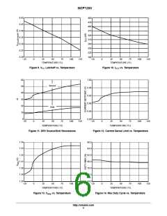
Internal
Fault
Flag
Fault is
Relaxed
Startup Phase
Fault Occurs Here
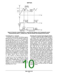
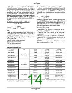
Figure 20. If the fault is relaxed during the VCC natural fall down sequence, the IC automatically resumes.
If the fault persists when VCC reached UVLOL, then the controller cuts everything off until recovery.
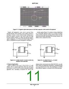
Calculating the V Capacitor
As the above section describes, the fall down sequence
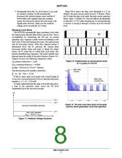
Protecting the Controller Against Negative Spikes
As with any controller built upon a CMOS technology, it
is the designer’s duty to avoid the presence of negative
spikes on sensitive pins. Negative signals have the bad habit
to forward bias the controller substrate and induce erratic
behaviors. Sometimes, the injection can be so strong that
internal parasitic SCRs are triggered, engendering
irremediable damages to the IC if they are a low impedance
CC
depends upon the V level: how long does it take for the
CC
V
CC
line to go from 11.4 V to 9.8 V? The required time
depends on the startup sequence of your system, i.e. when
you first apply the power to the IC. The corresponding
transient fault duration due to the output capacitor charging
must be less than the time needed to discharge from 11.4 V
to 9.8 V, otherwise the supply will not properly start. The test
consists in either simulating or measuring in the lab how
much time the system takes to reach the regulation at full
load. Let’s suppose that this time corresponds to 6ms.
path is offered between V and GND. If the current sense
CC
pin is often the seat of such spurious signals, the
high−voltage pin can also be the source of problems in
certain circumstances. During the turn−off sequence, e.g.
when the user unplugs the power supply, the controller is still
Therefore a V
fall time of 10 ms could be well
CC
appropriated in order to not trigger the overload detection
circuitry. If the corresponding IC consumption, including
the MOSFET drive, establishes at 1.5 mA, we can calculate
the required capacitor using the following formula:
DV @ C
fed by its V capacitor and keeps activating the MOSFET
CC
ON and OFF with a peak current limited by Rsense.
Unfortunately, if the quality coefficient Q of the resonating
network formed by Lp and Cbulk is low (e.g. the MOSFET
Rdson + Rsense are small), conditions are met to make the
circuit resonate and thus negatively bias the controller. Since
we are talking about ms pulses, the amount of injected
charge (Q = I x t) immediately latches the controller which
Dt +
, with DV = 2V. Then for a wanted Dt of 10 ms,
i
C equals 8 mF or 10 mF for a standard value. When an
overload condition occurs, the IC blocks its internal
circuitry and its consumption drops to 350 mA typical. This
brutally discharges its V capacitor. If this V capacitor
CC
CC
appends at V = 9.8 V and it remains stuck until V
CC
CC
is of sufficient value, its stored energy damages the
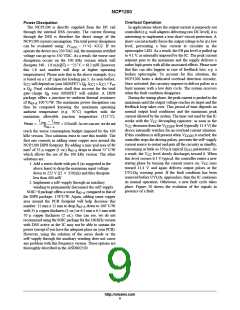
controller. Figure 21 depicts a typical negative shot
reaches 6.5 V: we are in latchoff phase. Again, using the
calculated 10 mF and 350 mA current consumption, this
latchoff phase lasts: 109 ms.
occurring on the HV pin where the brutal V discharge
CC
testifies for latchup.
http://onsemi.com
10

 ONSEMI [ ONSEMI ]