NCP1117, NCV1117
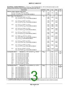
MAXIMUM RATINGS
Rating
Symbol
Value
20
Unit
V
Input Voltage (Note 1)
V
in
Output Short Circuit Duration (Notes 2 and 3)
−
Infinite
−
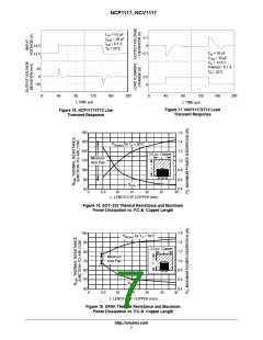
Power Dissipation and Thermal Characteristics
Case 318H (SOT−223)
Power Dissipation (Note 2)
P
D
Internally Limited
W
Thermal Resistance, Junction−to−Ambient, Minimum Size Pad
Thermal Resistance, Junction−to−Case
Case 369A (DPAK)
R
160
15
°C/W
°C/W
q
JA
JC
R
q
Power Dissipation (Note 2)
Internally Limited
W
P
D
Thermal Resistance, Junction−to−Ambient, Minimum Size Pad
Thermal Resistance, Junction−to−Case
67
°C/W
°C/W
R
q
JA
JC
6.0
R
q
Maximum Die Junction Temperature Range
Storage Temperature Range
TJ
−55 to 150
−65 to 150
°C
°C
°C
Tstg
Operating Ambient Temperature Range
T
A
NCP1117
NCV1117
0 to +125
−40 to +125
Stresses exceeding Maximum Ratings may damage the device. Maximum Ratings are stress ratings only. Functional operation above the
Recommended Operating Conditions is not implied. Extended exposure to stresses above the Recommended Operating Conditions may affect
device reliability.
1. This device series contains ESD protection and exceeds the following tests:
Human Body Model 2000 V per MIL−STD−883, Method 3015.
Machine Model Method 200 V.
2. Internal thermal shutdown protection limits the die temperature to approximately 175°C. Proper heatsinking is required to prevent activation.
The maximum package power dissipation is:
T
* T
J(max)
A
P
D
+
R
in
qJA
3. The regulator output current must not exceed 1.0 A with V greater than 12 V.
http://onsemi.com
2

 ONSEMI [ ONSEMI ]