NCP1117, NCV1117
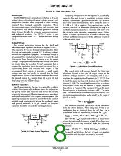
Protection Diodes
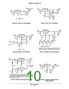
The second condition is that the ground end of R2 should be
connected directly to the load. This allows true Kelvin
sensing where the regulator compensates for the voltage
drop caused by wiring resistance RW −.
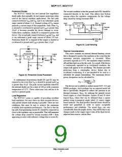
The NCP1117 family has two internal low impedance
diode paths that normally do not require protection when
used in the typical regulator applications. The first path
connects between V and V , and it can withstand a peak
out
in
surge current of about 15 A. Normal cycling of V cannot
Input
RW+ Output
in
3
2
NCP1117
XTA
generate a current surge of this magnitude. Only when V
in
+
Remote
Load
is shorted or crowbarred to ground and C is greater than
C
out
out
+
R1
1
C
in
50 mF, it becomes possible for device damage to occur.
R2
Under these conditions, diode D1 is required to protect the
device. The second path connects between C and V , and
adj
out
it can withstand a peak surge current of about 150 mA.
Protection diode D2 is required if the output is shorted or
RW−
crowbarred to ground and C is greater than 1.0 mF.
adj
Figure 23. Load Sensing
D1
Thermal Considerations
1N4001
This series contains an internal thermal limiting circuit
that is designed to protect the regulator in the event that the
maximum junction temperature is exceeded. When
activated, typically at 175°C, the regulator output switches
off and then back on as the die cools. As a result, if the device
is continuously operated in an overheated condition, the
output will appear to be oscillating. This feature provides
protection from a catastrophic device failure due to
accidental overheating. It is not intended to be used as a
substitute for proper heatsinking. The maximum device
power dissipation can be calculated by:
Input
C
Output
3
NCP1117
XTA
2
+
+
D2
1N4001
R1
C
in
out
1
+
C
adj
R2
Figure 22. Protection Diode Placement
A combination of protection diodes D1 and D2 may be
required in the event that V is shorted to ground and C
is greater than 50 mF. The peak current capability stated for
the internal diodes are for a time of 100 ms with a junction
temperature of 25°C. These values may vary and are to be
used as a general guide.
T
* T
A
J(max)
P
+
D
in
adj
R
qJA
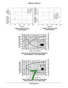
The devices are available in surface mount SOT−223 and
DPAK packages. Each package has an exposed metal tab
that is specifically designed to reduce the junction to air
thermal resistance, R , by utilizing the printed circuit
qJA
board copper as a heat dissipater. Figures 18 and 19 show
Load Regulation
typical R
values that can be obtained from a square
The NCP1117 series is capable of providing excellent
load regulation; but since these are three terminal devices,
only partial remote load sensing is possible. There are two
conditions that must be met to achieve the maximum
available load regulation performance. The first is that the
top side of programming resistor R1 should be connected as
close to the regulator case as practicable. This will minimize
the voltage drop caused by wiring resistance RW + from
appearing in series with reference voltage that is across R1.
qJA
pattern using economical single sided 2.0 ounce copper
board material. The final product thermal limits should be
tested and quantified in order to insure acceptable
performance and reliability. The actual R
can vary
qJA
considerably from the graphs shown. This will be due to any
changes made in the copper aspect ratio of the final layout,
adjacent heat sources, and air flow.
http://onsemi.com
9

 ONSEMI [ ONSEMI ]