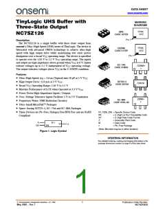
NC7SZ126
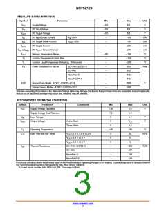
ABSOLUTE MAXIMUM RATINGS
Symbol
Parameter
Min
−0.5
−0.5
−0.5
−
Max
6.5
Unit
V
V
CC
Supply Voltage
V
IN
DC Input Voltage
6.5
V
V
DC Output Voltage
DC Input Diode Current
DC Output Diode Current
DC Output Current
6.5
V
OUT
I
V
< 0 V
−50
−50
50
mA
mA
mA
mA
°C
IK
IN
I
V
< 0 V
−
OK
OUT
I
−
OUT
I
or I
DC V or Ground Current
−
50
CC
GND
CC
T
STG
Storage Temperature Range
−65
−
+150
+150
+260
390
332
812
812
2000
1000
T
J
Junction Temperature Under Bias
°C
T
Junction Lead Temperature (Soldering, 10 Seconds)
Power Dissipation in Still Air
SC−74A / SOT23−5
−
°C
L
P
D
−
mW
SC−88A
−
MicroPak−6
MicroPak2ꢀ−6
−
−
ESD
Human Body Model, JEDEC: JESD22−A114
Charge Device Model, JEDEC: JESD22−C101
−
V
−
Stresses exceeding those listed in the Maximum Ratings table may damage the device. If any of these limits are exceeded, device functionality
should not be assumed, damage may occur and reliability may be affected.
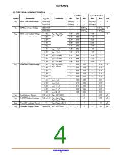
RECOMMENDED OPERATING CONDITIONS
Symbol
Parameter
Supply Voltage Operating
Supply Voltage Data Retention
Input Voltage
Conditions
Min
1.65
1.5
0
Max
5.5
5.5
5.5
Unit
V
CC
V
V
IN
V
V
V
OUT
Output Voltage
Active State
Three−State
0
V
CC
0
5.5
+85
20
T
A
Operating Temperature
Input Rise and Fall Times
−40
0
°C
t , t
V
CC
V
CC
V
CC
= 1.8 V, 2.5 V 0.2 V
= 3.3 V 0.3 V
ns/V
r
f
0
10
= 5.0 V 0.5 V
0
5
ꢀ
Thermal Resistance
SC−74A / SOT23−5
SC−88A
−
320
377
154
154
°C/W
JA
−
MicroPak−6
−
MicroPak2−6
−
Functional operation above the stresses listed in the Recommended Operating Ranges is not implied. Extended exposure to stresses beyond
the Recommended Operating Ranges limits may affect device reliability.
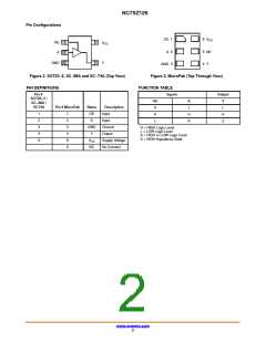
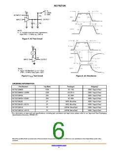
1. Unused inputs must be held HIGH or LOW. They may not float.
www.onsemi.com
3

 ONSEMI [ ONSEMI ]