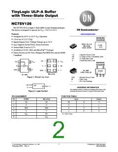
NC7SV126
MAXIMUM RATINGS
Symbol
Characteristics
Value
Unit
V
V
CC
DC Supply Voltage
DC Input Voltage
DC Output Voltage
−0.5 to +4.3
−0.5 to +4.3
V
IN
V
V
OUT
Active−Mode (High or Low State)
Tri−State Mode (Note 1)
−0.5 to V + 0.5
V
CC
−0.5 to +4.3
−0.5 to +4.3
Power−Down Mode (V = 0 V)
CC
I
DC Input Diode Current
V
< GND
< GND
−50
−50
mA
mA
mA
mA
°C
IK
IN
I
DC Output Diode Current
V
OUT
OK
I
DC Output Source/Sink Current
DC Supply Current per Supply Pin or Ground Pin
Storage Temperature Range
50
OUT
I
or I
GND
STG
50
CC
T
−65 to +150
260
T
Lead Temperature, 1 mm from Case for 10 Seconds
Junction Temperature Under Bias
Thermal Resistance (Note 2)
°C
L
T
+150
°C
J
q
SC−88A
MicroPak
377
154
°C/W
JA
P
D
Power Dissipation in Still Air
SC−88A
MikroPak
332
812
mW
MSL
Moisture Sensitivity
Level 1
−
−
V
F
R
Flammability Rating
Oxygen Index: 28 to 34
UL 94 V−0 @ 0.125 in
V
ESD
ESD Withstand Voltage (Note 3)
Human Body Model
Charged Device Model
2000
1000
I
Latchup Performance (Note 4)
100
mA
Latchup
Stresses exceeding those listed in the Maximum Ratings table may damage the device. If any of these limits are exceeded, device functionality
should not be assumed, damage may occur and reliability may be affected.
1. Applicable to devices with outputs that may be tri−stated.
2. Measured with minimum pad spacing on an FR4 board, using 10 mm−by−1 inch, 2 ounce copper trace no air flow per JESD51−7.
3. HBM tested to EIA / JESD22−A114−A. CDM tested to JESD22−C101−A. JEDEC recommends that ESD qualification to EIA/JESD22−A115A
(Machine Model) be discontinued.
4. Tested to EIA/JESD78 Class II.
RECOMMENDED OPERATING CONDITIONS
Symbol
Parameter
Min
0.9
0
Max
3.6
Unit
V
V
CC
Positive DC Supply Voltage
DC Input Voltage
V
IN
3.6
V
V
OUT
DC Output Voltage
Active−Mode (High or Low State)
Tri−State Mode (Note 1)
0
0
0
V
CC
3.6
3.6
Power−Down Mode (V = 0 V)
CC
T
Operating Temperature Range
−40
+85
10
°C
A
t , t
r
Input Transition Rise and Fall Time
V = 3.3 V 0.3 V
CC
0
ns/V
f
Functional operation above the stresses listed in the Recommended Operating Ranges is not implied. Extended exposure to stresses beyond
the Recommended Operating Ranges limits may affect device reliability.
www.onsemi.com
2

 ONSEMI [ ONSEMI ]