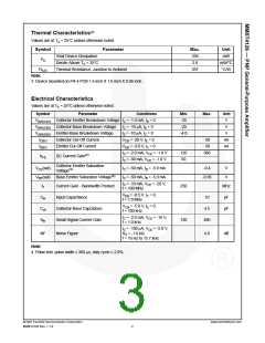
Thermal Characteristics(3)
Values are at TA = 25°C unless otherwise noted.
Symbol
PD
Parameter
Max.
350
2.8
Unit
mW
Total Device Dissipation
Derate Above TA = 25°C
mW/°C
°C/W
RθJA
Thermal Resistance, Junction to Ambient
357
Note:
3. Device mounted on FR-4 PCB 1.6 inch X 1.6 inch X 0.06 inch.
Electrical Characteristics
Values are at TA = 25°C unless otherwise noted.
Symbol
Parameter
Conditions
Min.
-25
Max.
Unit
V
V(BR)CEO Collector-Emitter Breakdown Voltage IC = -1.0 mA, IB = 0
V(BR)CBO Collector-Base Breakdown Voltage
V(BR)EBO Emitter-Base Breakdown Voltage
IC = -10 μA, IE = 0
-25
V
IE = -10 μA, IC = 0
-4.0
V
ICBO
IEBO
Collector Cut-Off Current
Emitter Cut-Off Current
VCB = -20 V, IE = 0
-50
-50
360
nA
nA
VEB = -3.0 V, IC = 0
IC = -2.0 mA, VCE = -1.0 V
IC = -50 mA, VCE = -1.0 V
120
60
hFE
DC Current Gain(4)
Collector-Emitter Saturation
Voltage(4)
VBE(sat) Base-Emitter Saturation Voltage(4)
VCE(sat)
IC = -50 mA, IB = -5.0 mA
-0.4
V
V
IC = -50 mA, IB = -5.0 mA
-0.95
IC = -10 mA, VCE = -20 V,
f = 100 MHz
fT
Current Gain - Bandwidth Product
Input Capacitance
250
120
MHz
VEB = -0.5 V, IC = 0,
f = 1.0 MHz
Cib
Ccb
hfe
10
4.5
480
pF
pF
VCB = -5.0 V, IE = 0,
f = 100 kHz
Collector-Base Capcitance
Small-Signal Current Gain
IC = -2.0 mA, VCE = -10 V,
f = 1.0 kHz
IC = -100 μA, VCE = -5.0 V,
RS = -1.0 kΩ,
f = 10 Hz to 15.7 kHz
NF
Noise Figure
4.0
dB
Note:
4. Pulse test: pulse width ≤ 300 μs, duty cycle ≤ 2.0%.
©1997 Fairchild Semiconductor Corporation
MMBT4126 Rev. 1.1.0
www.fairchildsemi.com
2

 ONSEMI [ ONSEMI ]