ELECTRICAL CHARACTERISTICS (T = 25°C unless otherwise noted)
C
Characteristic
Symbol
Min
Typical
Max
Unit
OFF CHARACTERISTICS
Emitter Cutoff Current
I
—
—
—
—
100
100
µAdc
µAdc
EBO
(V
CE
= 5 Vdc, I = 0)
C
Collector Cutoff Current
(V = 250 Vdc, V
I
CEX
= 1.5 Vdc)
CE BE(off)
SECOND BREAKDOWN
Second Breakdown Collector Current with Base Forward Biased
I
Adc
S/b
(V
CE
(V
CE
= 50 Vdc, t = 1 s (non–repetitive)
= 80 Vdc, t = 1 s (non–repetitive)
4.0
2.25
—
—
—
—
ON CHARACTERISTICS
DC Current Gain
h
FE
(I = 8 Adc, V
= 5 Vdc)
(I = 16 Adc, I = 5 Adc)
25
8
—
—
75
—
C
CE
C
B
Base–Emitter On Voltage
(I = 8 Adc, V = 5 Vdc)
V
—
—
2.2
Vdc
Vdc
BE(on)
C
CE
Collector–Emitter Saturation Voltage
(I = 8 Adc, I = 0.8 Adc)
V
CE(sat)
—
—
—
—
1.4
4
C
B
(I = 16 Adc, I = 3.2 Adc)
C
B
DYNAMIC CHARACTERISTICS
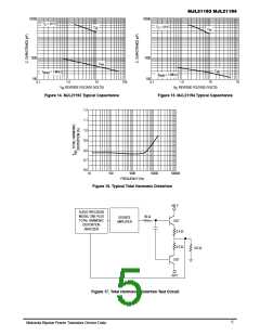
Total Harmonic Distortion at the Output
T
HD
%
V
RMS
= 28.3 V, f = 1 kHz, P
= 100 W
RMS
h
LOAD
FE
unmatched
—
0.8
—
(Matched pair h
FE
= 50 @ 5 A/5 V)
h
FE
matched
—
4
0.08
—
—
—
Current Gain Bandwidth Product
(I = 1 Adc, V = 10 Vdc, f
f
T
MHz
pF
= 1 MHz)
C
CE test
Output Capacitance
(V = 10 Vdc, I = 0, f
C
—
—
500
ob
= 1 MHz)
CB test
E
(1)
Pulse Test: Pulse Width = 300 µs, Duty Cycle ≤2%
PNP MJL21193
NPN MJL21194
6.5
8.0
7.0
V
= 10 V
CE
6.0
5.5
5.0
4.5
10 V
6.0
5.0
4.0
5 V
V
= 5 V
CE
3.0
2.0
1.0
4.0
3.5
T
= 25
= 1 MHz
°
C
T
= 25
= 1 MHz
°
C
J
J
f
f
test
test
3.0
0.1
0
0.1
1.0
10
1.0
10
I
COLLECTOR CURRENT (AMPS)
I COLLECTOR CURRENT (AMPS)
C
C
Figure 1. Typical Current Gain
Bandwidth Product
Figure 2. Typical Current Gain
Bandwidth Product
2
Motorola Bipolar Power Transistor Device Data

 ONSEMI [ ONSEMI ]