MC34071,2,4,A MC33071,2,4,A
values of feedback resistances (lower current DACs). This
minimum current sink capability, typically to an output
input pole can be compensated for by creating a feedback
zero with a capacitance across the feedback resistance, if
necessary, to reduce overshoot. For 2.0 kΩ of feedback
resistance, the MC34071 series can settle to within 1/2 LSB
of 8 bits in 1.0 µs, and within 1/2 LSB of 12–bits in 2.2 µs
for a 10 V step. In a inverting unity gain fast settling
configuration, the symmetrical slew rate is ±13 V/µs. In the
classic noninverting unity gain configuration, the output
positive slew rate is +10 V/µs, and the corresponding
negative slew rate will exceed the positive slew rate as a
function of the fall time of the input waveform.
Since the bipolar input device matching characteristics
are superior to that of JFETs, a low untrimmed maximum
offset voltage of 3.0 mV prime and 5.0 mV downgrade can
be economically offered with high frequency performance
characteristics. This combination is ideal for low cost
precision, high speed quad op amp applications.
voltage of (V +1.8 V). In single supply applications the
EE
output can directly source or sink base current from a
common emitter NPN transistor for fast high current
switching applications.
In addition, the all NPN transistor output stage is
inherently fast, contributing to the bipolar amplifier’s high
gain bandwidth product and fast settling capability. The
associated high frequency low output impedance (30 Ω typ
@ 1.0 MHz) allows capacitive drive capability from 0 pF to
10,000 pF without oscillation in the unity closed loop gain
configuration. The 60° phase margin and 12 dB gain margin
as well as the general gain and phase characteristics are
virtually independent of the source/sink output swing
conditions. This allows easier system phase compensation,
since output swing will not be a phase consideration. The
high frequency characteristics of the MC34071 series also
allow excellent high frequency active filter capability,
especially for low voltage single supply applications.
Although the single supply specifications is defined at
5.0 V, these amplifiers are functional to 3.0 V @ 25°C
although slight changes in parametrics such as bandwidth,
slew rate, and DC gain may occur.
The all NPN output stage, shown in its basic form on the
equivalent circuit schematic, offers unique advantages over
the more conventional NPN/PNP transistor Class AB
output stage. A 10 kΩ load resistance can swing within 1.0
V of the positive rail (V ), andwithin0.3Vofthenegative
CC
rail(V ),providinga28.7V swingfrom±15Vsupplies.
If power to this integrated circuit is applied in reverse
polarity or if the IC is installed backwards in a socket, large
unlimited current surges will occur through the device that
may result in device destruction.
EE pp
This large output swing becomes most noticeable at lower
supply voltages.
The positive swing is limited by the saturation voltage of
thecurrentsourcetransistorQ , andV oftheNPNpullup
Special static precautions are not necessary for these
bipolar amplifiers since there are no MOS transistors on
the die.
7
BE
transistorQ ,andthevoltagedropassociatedwiththeshort
17
circuit resistance, R . The negative swing is limited by the
7
saturation voltage of the pull–down transistor Q , the
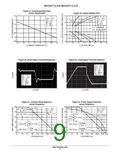
As with most high frequency amplifiers, proper lead
dress, component placement, and PC board layout should
be exercised for optimum frequency performance. For
example, long unshielded input or output leads may result in
unwanted input–output coupling. In order to preserve the
relatively low input capacitance associated with these
amplifiers, resistors connected to the inputs should be
immediatelyadjacent to the input pin to minimize additional
stray input capacitance. This not only minimizes the input
pole for optimum frequency response, but also minimizes
extraneous “pick up” at this node. Supply decoupling with
adequatecapacitanceimmediatelyadjacenttothesupplypin
is also important, particularly over temperature, since many
types of decoupling capacitors exhibit great impedance
changes over temperature.
The output of any one amplifier is current limited and thus
protected from a direct short to ground. However, under
such conditions, it is important not to allow the device to
exceed the maximum junction temperature rating. Typically
for ±15 V supplies, any one output can be shorted
continuously to ground without exceeding the maximum
temperature rating.
16
voltage drop I R , and the voltage drop associated with
L 6
resistance R , where I is the sink load current. For small
7
L
valued sink currents, the above voltage drops are negligible,
allowing the negative swing voltage to approach within
millivolts of V . For large valued sink currents (>5.0 mA),
EE
diode D3 clamps the voltage across R , thus limiting the
6
negative swing to the saturation voltage of Q , plus the
16
forward diode drop of D3 (≈V +1.0 V). Thus for a given
EE
supplyvoltage, unprecedentedpeak–to–peakoutputvoltage
swing is possible as indicated by the output swing
specifications.
If the load resistance is referenced to V
instead of
CC
ground for single supply applications, the maximum
possible output swing can be achieved for a given supply
voltage. For light load currents, the load resistance will pull
the output to V
during the positive swing and the output
CC
will pull the load resistance near ground during the negative
swing. The load resistance value should be much less than
that of the feedback resistance to maximize pull up
capability.
Because the PNP output emitter–follower transistor has
been eliminated, the MC34071 series offers a 20 mA
http://onsemi.com
11

 ONSEMI [ ONSEMI ]