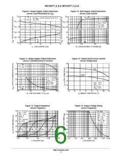
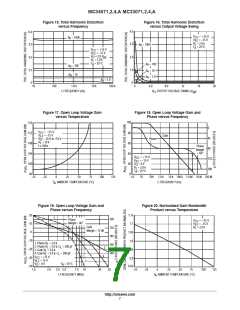
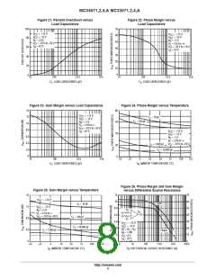
MC34071,2,4,A MC33071,2,4,A
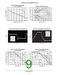
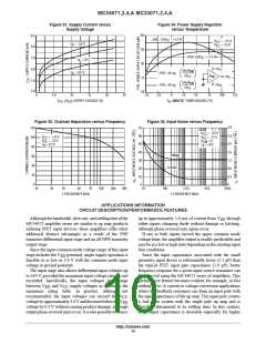
Figure 33. Supply Current versus
Supply Voltage
Figure 34. Power Supply Rejection
versus Temperature
105
95
85
75
65
9.0
8.0
7.0
6.0
–PSR (∆V = +1.5 V)
EE
V
V
EE
= +15 V
= –15 V
CC
T = –55°C
A
(∆V = +1.5 V)
+PSR
CC
T = 25°C
A
∆V
CC
∆V /A
O
DM
T = 125°C
A
–
+PSR = 20 Log
–PSR = 20 Log
∆V
A
CC
DM
∆V
O
+
5.0
4.0
∆V /A
O
DM
∆V
EE
∆V
EE
0
5.0
10
15
20
25
–55
–25
0
25
50
75
100
125
V
, |V |, SUPPLY VOLTAGE (V)
T , AMBIENT TEMPERATURE (°C)
A
CC EE
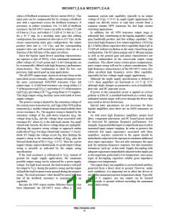
Figure 35. Channel Separation versus Frequency
Figure 36. Input Noise versus Frequency
2.8
120
100
80
60
40
20
0
70
V
= +15 V
= –15 V
= 0
CC
60
50
40
30
20
10
0
2.4
2.0
1.6
1.2
0.8
0.4
V
= +15 V
= –15 V
V
CC
EE
V
V
EE
CM
T = 25°C
T = 25°C
A
A
Voltage
Current
0
10
20
30
50
70
100
200
300
10
100
1.0 k
f, FREQUENCY (kHz)
10 k
100 k
f, FREQUENCY (kHz)
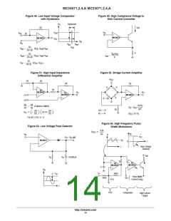
APPLICATIONS INFORMATION
CIRCUIT DESCRIPTION/PERFORMANCE FEATURES
Althoughthebandwidth, slewrate, andsettlingtimeofthe
MC34071 amplifier series are similar to op amp products
utilizing JFET input devices, these amplifiers offer other
additional distinct advantages as a result of the PNP
transistor differential input stage and an all NPN transistor
output stage.
up to approximately 5.0 mA of current from V through
EE
either inputs clamping diode without damage or latching,
although phase reversal may again occur.
If one or both inputs exceed the upper common mode
voltage limit, the amplifier output is readily predictable and
may be in a low or high state depending on the existing input
bias conditions.
Since the input common mode voltage range of this input
stage includes the V potential, single supply operation is
feasible to as low as 3.0 V with the common mode input
voltage at ground potential.
The input stage also allows differential input voltages up
to ±44 V, provided the maximum input voltage range is not
exceeded. Specifically, the input voltages must range
Since the input capacitance associated with the small
geometry input device is substantially lower (2.5 pF) than
the typical JFET input gate capacitance (5.0 pF), better
frequency response for a given input source resistance can
be achieved using the MC34071 series of amplifiers. This
performance feature becomes evident, for example, in fast
settling D–to–A current to voltage conversion applications
where the feedback resistance can form an input pole with
the input capacitance of the op amp. This input pole creates
a 2nd order system with the single pole op amp and is
therefore detrimental to its settling time. In this context,
lower input capacitance is desirable especially for higher
EE
between V
and V
supply voltages as shown by the
EE
maximum rating table. In practice, although not
recommended, the input voltages can exceed the V
CC
CC
voltagebyapproximately3.0VanddecreasebelowtheV
EE
voltage by 0.3 V without causing product damage, although
output phase reversal may occur. It is also possible to source
http://onsemi.com
10

 ONSEMI [ ONSEMI ]