MC14001B Series
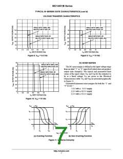
TYPICAL B−SERIES GATE CHARACTERISTICS (cont’d)
VOLTAGE TRANSFER CHARACTERISTICS
SINGLE INPUT NAND, AND
MULTIPLE INPUT NOR, OR
SINGLE INPUT NAND, AND
MULTIPLE INPUT NOR, OR
5.0
10
8.0
6.0
4.0
3.0
2.0
1.0
0
SINGLE INPUT NOR, OR
SINGLE INPUT NOR, OR
MULTIPLE INPUT NAND, AND
MULTIPLE INPUT NAND, AND
4.0
2.0
0
0
1.0
2.0
3.0
4.0
5.0
0
2.0
4.0
6.0
8.0
10
V , INPUT VOLTAGE (Vdc)
in
V , INPUT VOLTAGE (Vdc)
in
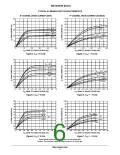
Figure 8. VDD = 5.0 Vdc
Figure 9. VDD = 10 Vdc
16
DC NOISE MARGIN
SINGLE INPUT NAND, AND
14
12
10
MULTIPLE INPUT NOR, OR
The DC noise margin is defined as the input voltage range
from an ideal “1” or “0” input level which does not produce
output state change(s). The typical and guaranteed limit
values of the input values V and V for the output(s) to
SINGLE INPUT NOR, OR
MULTIPLE INPUT NAND, AND
IL
IH
be at a fixed voltage V are given in the Electrical
O
8.0
6.0
Characteristics table. V and V are presented graphically
IL
IH
in Figure 11.
Guaranteed minimum noise margins for both the “1” and
“0” levels =
4.0
2.0
0
1.0 V with a 5.0 V supply
2.0 V with a 10.0 V supply
2.5 V with a 15.0 V supply
0
2.0
4.0
6.0
8.0
10
V , INPUT VOLTAGE (Vdc)
in
Figure 10. VDD = 15 Vdc
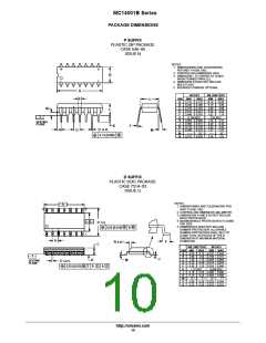
V
out
V
DD
V
out
V
DD
V
O
V
O
V
O
V
O
V
V
V
V
DD
DD
0
0
in
in
V
IL
V
IH
V
IL
V
IH
V
SS
= 0 VOLTS DC
(a) Inverting Function
(b) Non−Inverting Function
Figure 11. DC Noise Immunity
http://onsemi.com
7

 ONSEMI [ ONSEMI ]