LMV931, LMV932
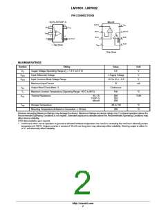
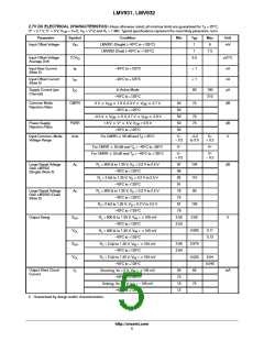
PIN CONNECTIONS
SC70−5/TSOP−5
Micro8
OUT A
V
CC
1
2
3
5
1
8
+IN
V
CC
A
− +
IN A−
OUT B
2
3
7
6
+
−
V
EE
B
4
IN A+
+
−
IN B−
−IN
OUTPUT
IN B+
4
5
V
(Top View)
EE
(Top View)
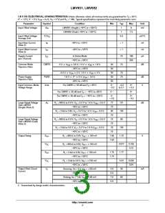
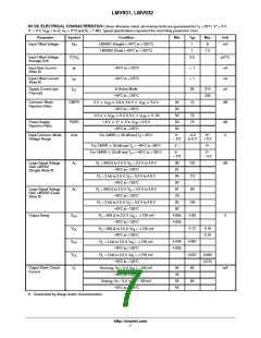
MAXIMUM RATINGS
Symbol
Rating
Value
Unit
V
V
S
Supply Voltage (Operating Range V = 1.8 V to 5.5 V)
5.5
S
V
Input Differential Voltage
$Supply Voltage
−0.5 to (V+) + 0.5
10
V
IDR
ICR
V
Input Common Mode Voltage Range
Maximum Input Current
V
mA
t
Output Short Circuit (Note 1)
Continuous
150
So
T
Maximum Junction Temperature (Operating Range −40°C to 85°C)
°C
J
q
Thermal Resistance:
SC−70
TSOP−5
Micro8
280
333
238
°C/W
JA
T
stg
Storage Temperature
−65 to 150
°C
°C
Mounting Temperature (Infrared or Convection v 30 sec)
260
Stresses exceeding Maximum Ratings may damage the device. Maximum Ratings are stress ratings only. Functional operation above the
Recommended Operating Conditions is not implied. Extended exposure to stresses above the Recommended Operating Conditions may
affect device reliability.
ESD data available upon request.
1. Continuous short−circuit operation to ground at elevated ambient temperature can result in exceeding the maximum allowed junction
temperature of 150°C. Output currents in excess of 45 mA over long term may adversely affect reliability. Shorting output to either V+
or V− will adversely affect reliability.
http://onsemi.com
2

 ONSEMI [ ONSEMI ]