FDN336P
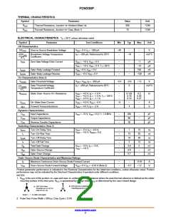
THERMAL CHARACTERISTICS
Symbol
Parameter
Value
250
75
Unit
°C/W
°C/W
R
Thermal Resistance, Junction−to−Ambient (Note 1a)
Thermal Resistance, Junction−to−Case (Note 1)
θ
JA
JC
R
θ
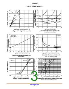
ELECTRICAL CHARACTERISTICS T = 25°C unless otherwise noted
A
Symbol
Parameter
Test Conditions
Min
Typ
Max
Unit
Off Characteristics
BV
Drain to Source Breakdown Voltage
V
I
= 0 V, I = −250 ꢂ A
−20
−
−
−
V
DSS
GS
D
Breakdown Voltage Temperature
Coefficient
= −250 ꢂ A, Referenced to 25°C
−
−16
mV/°C
ꢃ BVDSS
ꢃ TJ
D
I
Zero Gate Voltage Drain Current
V
V
V
V
= −16 V, V = 0 V
−
−
−
−
−
−
−
−
−1
−10
100
−100
ꢂ A
ꢂ A
nA
nA
DSS
DS
GS
= −16 V, V = 0 V, T = 55°C
DS
GS
GS
GS
J
I
Gate−Body Leakage Forward
Gate−Body Leakage Reverse
= 8 V, V = 0 V
DS
GSSF
I
= −8 V, V = 0 V
DS
GSSR
On Characteristics (Note 2)
V
GS(th)
Gate Threshold Voltage
V
DS
= V , I = −250 ꢂ A
−0.4
−0.9
−1.5
V
GS D
Gate Threshold Voltage
Temperature Coefficient
I = −250 ꢂA, Referenced to 25°C
D
−
3
−
mV/°C
ꢃ VGS(th)
ꢃ TJ
R
Static Drain−Source On−Resistance
V
GS
V
GS
V
GS
= −4.5 V, I = −1.3 A
−
−
−
0.122
0.18
0.19
0.2
0.32
0.27
ꢀ
DS(on)
D
= −4.5 V, I = −1.3 A, T = 125°C
D
J
= −2.5 V, I = −1.1 A
D
I
On−State Drain Current
V
= −4.5 V, V = −5 V
−5
−
−
−
A
S
D(on)
GS
DS
DS
g
FS
Forward Transconductance
V
= −4.5 V, I = −2 A
4
D
Dynamic Characteristics
C
Input Capacitance
V
DS
= −10 V, V = 0 V, f = 1.0 MHz
−
−
−
330
80
−
−
−
pF
pF
pF
iss
GS
C
Output Capacitance
oss
C
Reverse Transfer Capacitance
35
rss
Switching Characteristics (Note 2)
t
Turn−On Delay Time
Turn−On Rise Time
Turn−Off Delay Time
Turn−Off Fall Time
Total Gate Change
Gate−Source Change
Gate−Drain Change
V
V
= −5 V, I = −0.5 A,
−
−
−
−
−
−
−
7
15
22
26
12
5
ns
ns
d(on)
DD
GS
D
= −4.5 V, R
= 6 Ω
GEN
t
r
12
16
5
t
ns
d(off)
t
f
ns
Q
V
DS
V
GS
= −10 V, I = −2 A,
3.6
0.8
0.7
nC
nC
nC
g
D
= −4.5 V
Q
−
gs
gd
Q
−
Drain−Source Diode Characteristics and Maximum Ratings
Maximum Continuous Drain–Source Diode Forward Current
Drain−Source Diode Forward Voltage = 0 V, I = −0.42 A (Note 2)
I
−
−
−
−0.42
−1.2
A
V
S
V
SD
V
GS
−0.7
S
Product parametric performance is indicated in the Electrical Characteristics for the listed test conditions, unless otherwise noted. Product
performance may not be indicated by the Electrical Characteristics if operated under different conditions.
NOTES:
1. R
is the sum of the junction−to−case and case−to−ambient thermal resistance where the case thermal reference is defined as the solder
ꢄ
JA
mounting surface of the drain pins. R
is guaranteed by design while R
is determined by the user’s board design.
ꢄ
ꢄ
JC
CA
b) 270°C/W on a minimum
a) 250°C/W when
2
mounting pad of 2 oz. Cu.
mounted on a 0.02 in
Pad of 2 oz. Cu.
Scale 1 : 1 on letter size paper
2. Pulse Test: Pulse Width ≤ 300 ꢂ s, Duty Cycle ≤ 2.0%
www.onsemi.com
2

 ONSEMI [ ONSEMI ]