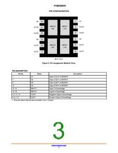
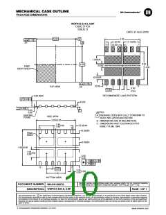
MECHANICAL CASE OUTLINE
PACKAGE DIMENSIONS
WDFN12 5x4.5, 0.8P
CASE 511CS
ISSUE O
DATE 31 AUG 2016
5.00
A
B
4.45
(0.40)
(0.25)
0.10 C
2.10(4X)
7
2X
12
1.00(4X)
(0.50)
3.50
4.50
PIN#1
IDENT AREA
4.80
(0.50)2X
0.10 C
1
0.80
(0.65)
6
TOP VIEW
2X
0.40
(12x)
RECOMMENDED LAND PATTERN
0.80 MAX
0.10 C
(0.20)
0.08 C
0.05
C
NOTES:
0.00
A. PACKAGE DOES NOT FULLY CONFORM TO
JEDEC MO−229 REGISTRATION
B. DIMENSIONS ARE IN MILLIMETERS.
C. DIMENSIONS AND TOLERANCES PER
ASME Y14.5M, 1994.
SEATING
SIDE VIEW
PLANE
0.05
5.00
1.95
(4X)
(0.35)4X
(0.50)2X
1.85
1
6
PIN#1
IDENT
(0.50)2X
0.05
4.50
1.05
0.95
(4X)
0.55
0.45
0.10 C A B
0.05
C
7
12
0.80
2.40
0.35
0.25
(12X)
BOTTOM VIEW
Electronic versions are uncontrolled except when accessed directly from the Document Repository.
Printed versions are uncontrolled except when stamped “CONTROLLED COPY” in red.
DOCUMENT NUMBER:
DESCRIPTION:
98AON13607G
WDFN12 5X4.5, 0.8P
PAGE 1 OF 1
ON Semiconductor and
are trademarks of Semiconductor Components Industries, LLC dba ON Semiconductor or its subsidiaries in the United States and/or other countries.
ON Semiconductor reserves the right to make changes without further notice to any products herein. ON Semiconductor makes no warranty, representation or guarantee regarding
the suitability of its products for any particular purpose, nor does ON Semiconductor assume any liability arising out of the application or use of any product or circuit, and specifically
disclaims any and all liability, including without limitation special, consequential or incidental damages. ON Semiconductor does not convey any license under its patent rights nor the
rights of others.
© Semiconductor Components Industries, LLC, 2019
www.onsemi.com

 ONSEMI [ ONSEMI ]