FDMA507PZ
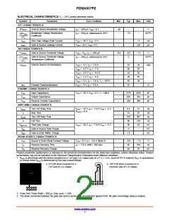
ELECTRICAL CHARACTERISTICS (T = 25°C unless otherwise noted)
J
Symbol
Parameter
Test Condition
Min
Typ
Max
Unit
OFF CHARACTERISTICS
BV
Drain to Source Breakdown Voltage
I
I
= −250 mA, V = 0 V
−20
−
−
−
−
V
DSS
D
GS
Breakdown Voltage Temperature
Coefficient
= −250 mA, referenced to 25°C
−12
mV/°C
DBVDSS
DTJ
D
I
Zero Gate Voltage Drain Current
Gate to Source Leakage Current
V
V
= −16 V, V = 0 V
−
−
−
−
−1
10
mA
mA
DSS
GSS
DS
GS
I
= 8 V, V = 0 V
DS
GS
ON CHARACTERISTICS
V
Gate to Source Threshold Voltage
V
I
= V , I = −250 mA
−0.4
−
−0.5
3
−1.5
−
V
GS(th)
GS
DS D
Gate to Source Threshold Voltage
Temperature Coefficient
= −250 mA, referenced to 25°C
mV/°C
DVGS(th)
DTJ
D
r
Drain to Source On Resistance
Forward Transconductance
V
GS
V
GS
V
GS
V
GS
V
GS
V
DS
= −5 V, I = −7.8 A
−
−
−
−
−
−
19
20
24
29
26
33
24
25
35
45
34
−
mW
DS(on)
D
= −4.5 V, I = −7 A
D
= −2.5 V, I = −5.5 A
D
= −1.8 V, I = −4 A
D
= −5 V, I = −7.8 A, T = 125°C
D
J
g
FS
= −5 V, I = −7.8 A
S
D
DYNAMIC CHARACTERISTICS
C
Input Capacitance
V
DS
= −10 V, V = 0 V, f = 1 MHz
−
−
−
1515
265
2015
355
pF
pF
pF
iss
GS
C
oss
Output Capacitance
C
rss
Reverse Transfer Capacitance
240
360
SWITCHING CHARACTERISTICS
t
Turn−On Delay Time
Rise Time
V
R
= −10 V, I = −7.8 A V = −5 V,
−
−
−
−
−
−
−
6.4
14
192
96
30
2
13
25
307
154
42
−
ns
ns
d(on)
DD
D
GS
= 6 W
GEN
t
r
t
Turn−Off Delay Time
Fall Time
ns
d(off)
t
f
ns
Q
g(TOT)
Total Gate Charge
Gate to Source Gate Charge
Gate to Drain “Miller” Charge
V
= −10 V, I = −7.8 A V = −5 V
nC
nC
nC
DD
GS
D
GS
Q
Q
gs
gd
7.5
−
DRAIN−SOURCE CHARACTERISTICS
V
Source to Drain Diode Forward Voltage
Reverse Recovery Time
V
= 0 V, I = −2.0 A (Note 2)
−
−
−
−0.6
66
−1.2
106
70
V
SD
S
t
rr
I = −7.8 A, di/dt = 100 A/ms
F
ns
nC
Q
rr
Reverse Recovery Charge
44
Product parametric performance is indicated in the Electrical Characteristics for the listed test conditions, unless otherwise noted. Product
performance may not be indicated by the Electrical Characteristics if operated under different conditions.
2
1. R
is determined with the device mounted on a 1 in pad 2 oz copper pad on a 1.5 x 1.5 in. board of FR−4 material. R
is guaranteed
JC
q
q
JA
by design while R
is determined by the user’s board design.
q
CA
a. 52°C/W when mounted on a
b. 145°C/W when mounted on a
minimum pad of 2 oz copper
2
1 in pad of 2 oz copper
2. Pulse Test: Pulse Width < 300 ms, Duty cycle < 2.0%.
3. The diode connected between the gate and source serves only as protection against ESD. No gate overvoltage rating is implied.
www.onsemi.com
2

 ONSEMI [ ONSEMI ]