ADM1026
Serial Bus Interface
ADM1026 is powered down, unlike the data in the volatile
registers. Although referred to as read−only memory, the
EEPROM can be written to (as well as read from) via the
serial bus in exactly the same way as the other registers. The
main differences between the EEPROM and other registers
are:
• An EEPROM location must be blank before it can be
written to. If it contains data, it must first be erased.
• Writing to EEPROM is slower than writing to RAM.
• Writing to the EEPROM should be restricted because
its typical cycle life is 100,000 write operations, due to
the usual EEPROM wear−out mechanisms.
The EEPROM in the ADM1026 has been qualified for
two key EEPROM memory characteristics: memory cycling
endurance and memory data retention.
Endurance qualifies the ability of the EEPROM to be
cycled through many program, read, and erase cycles. In real
terms, a single endurance cycle is composed of four
independent, sequential events, as follows:
Control of the ADM1026 is carried out via the serial
system management bus (SMBus). The ADM1026 is
connected to this bus as a slave device, under the control of
a master device.
The ADM1026 has a 7−bit serial bus slave address. When
the device is powered on, it does so with a default serial bus
address. The 5 MSBs of the address are set to 01011, and the
2 LSBs are determined by the logical states of Pin 15
ADD/NTESTOUT. This pin is a three−state input that can be
grounded, connected to V , or left open−circuit to give
three different addresses.
CC
Table 2. Address Pin Truth Table
ADD Pin
A1
A0
GND
No Connect
0
1
0
0
0
1
V
CC
If ADD is left open−circuit, the default address is 0101110
(5Ch). ADD is sampled only at powerup on the first valid
SMBus transaction, so any changes made while the power
is on (and the address is locked) have no effect.
1. Initial page erase sequence
2. Read/verify sequence
3. Program sequence
4. Second read/verify sequence
The facility to make hardwired changes to device
addresses allows the user to avoid conflicts with other
devices sharing the same serial bus, for example if more than
one ADM1026 is used in a system.
In reliability qualification, every byte is cycled from 00h
to FFh until a first fail is recorded, signifying the endurance
limit of the EEPROM memory.
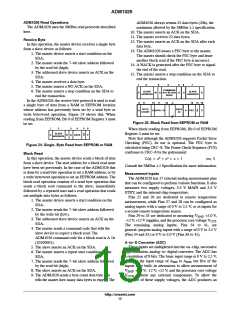
Retention quantifies the ability of the memory to retain its
programmed data over time. The EEPROM in the ADM1026
has been qualified in accordance with the formal JEDEC
Retention Lifetime Specification (A117) at a specific junction
General SMBus Timing
Figure 16 and Figure 17 show timing diagrams for general
read and write operations using the SMBus. The SMBus
specification defines specific conditions for different types
of read and write operations, which are discussed later in this
section. The general SMBus protocol* operates as follows:
1. The master initiates data transfer by establishing a
start condition, defined as a high−to−low transition
on the serial data line (SDA) while the serial clock
line SCL remains high. This indicates that a data
stream follows. All slave peripherals connected to
the serial bus respond to the start condition and
shift in the next 8 bits, consisting of a 7−bit slave
address (MSB first) and an R/W bit, which
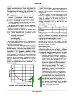
temperature (T = 55°C) to guarantee a minimum of 10 years
J
retention time. As part of this qualification procedure, the
EEPROM memory is cycled to its specified endurance limit
described above before data retention is characterized. This
means that the EEPROM memory is guaranteed to retain its
data for its full specified retention lifetime every time the
EEPROM is reprogrammed. Note that retention lifetime
based on an activation energy of 0.6 V derates with T , as
J
shown in Figure 15.
300
determine the direction of the data transfer, that is,
whether data is written to or read from the slave
device (0 = write, 1 = read).
250
200
150
100
The peripheral whose address corresponds to the
trans−mitted address responds by pulling the data
line low during the low period before the ninth
clock pulse, known as the acknowledge bit, and
holding it low during the high period of this clock
pulse. All other devices on the bus remain idle
while the selected device waits for data to be read
from or written to it. If the R/W bit is 0, the master
writes to the slave device. If the R/W bit is 1, the
master reads from the slave device.
50
0
110
40
50
60
70
80
90
JUNCTION TEMPERATURE (5C)
100
120
Figure 15. Typical EEPROM Memory Retention
http://onsemi.com
11

 ONSEMI [ ONSEMI ]