ADM1026
Functional Description
Chassis Intrusion
The ADM1026 is a complete system hardware monitor for
microprocessor−based systems. The device communicates
with the system via a serial system management bus. The
serial bus controller has a hardwired address line for device
selection (ADD, Pin 15), a serial data line for reading and
writing addresses and data (SDA, Pin 14), and an input line
for the serial clock (SCL, Pin 13). All control and
programming functions of the ADM1026 are performed over
the serial bus.
A chassis intrusion input (Pin 16) is provided to detect
unauthorized tampering with the equipment. This event is
latched in a battery−backed register bit.
Resets
The ADM1026 has two power−on reset outputs,
RESETMAIN and RESETSTBY, that are asserted when
3.3 V MAIN or 3.3 V STBY fall below the reset threshold.
These give a 180 ms reset pulse at powerup. RESETMAIN
also functions as an active−low RESET input.
Measurement Inputs
Fan Speed Control Outputs
Programmability of the analog and digital measurement
inputs makes the ADM1026 extremely flexible and
versatile. The device has an 8−bit A/D converter, and 17
analog measurement input pins that can be configured in
different ways.
Pins 25 and 26 are dedicated temperature inputs and may
be connected to the cathode and anode of a remote
temperature sensing diode.
Pins 27 and 28 may be configured as temperature inputs
and connected to a second temperature−sensing diode, or may
be reconfigured as analog inputs with a range of 0 V to 2.5 V.
Pins 29 to 33 are dedicated analog inputs with on−chip
The ADM1026 has two outputs intended to control fan
speed, though they can also be used for other purposes.
Pin 18 is an open drain, Pulse Width Modulated (PWM)
output with a programmable duty cycle and an output
frequency of 75 Hz. Pin 23 is connected to the output of an
on−chip, 8−bit, digital−to−analog converter with an output
range of 0 V to 2.5 V.
Either or both of these outputs may be used to implement
a temperature−controlled fan by controlling the speed of a
fan using the temperature measured by the on−chip
temperature sensor or remote temperature sensors.
attenuators configured to monitor V , +5.0 V, −12 V,
BAT
Internal Registers
Table 1 describes the principal registers of the ADM1026.
For more detailed information, see Table 8 to Table 121.
+12 V, and the processor core voltage V , respectively.
CCP
Pins 34 to 41 are general−purpose analog inputs with a
range of 0 V to 2.5 V or 0 V to 3.0 V. These are mainly
intended for monitoring SCSI termination voltages, but may
be used for other purposes.
Table 1. Principle Registers
Type
Description
The ADC also accepts input from an on−chip band gap
temperature sensor that monitors system ambient
temperature.
Address
Pointer
Contains the address that selects one of
the other internal registers. When writing to
the ADM1026, the first byte of data is
always a register address, and is written to
the address pointer register.
In addition, the ADM1026 monitors the supply from
which it is powered, 3.3 V STBY, so there is no need for a
separate pin to monitor the power supply voltage.
The ADM1026 has eight pins that are general−purpose
logic I/O pins (Pins 1, 2, and 43 to 48), a pin that can be
configured as GPIO or as a bidirectional thermal interrupt
(THERM) pin (Pin 42), and eight pins that can be configured
for fan speed measurement or as general−purpose logic pins
(Pins 3 to 6 and Pins 9 to 12).
Configuration
Registers
Provide control and configuration for
various operating parameters.
Fan Divisor
Registers
Contain counter prescaler values for fan
speed measurement.
DAC/PWM
Control
Registers
Contain speed values for PWM and DAC
fan drive outputs.
GPIO
Configuration
Registers
Configure the GPIO pins as input or output
and for signal polarity.
Sequential Measurement
Value and
Limit
Store the results of analog voltage inputs,
temperature, and fan speed measurements,
along with their limit values.
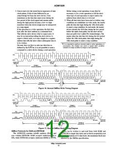
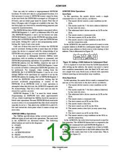
When the ADM1026 monitoring sequence is started, it
cycles sequentially through the measurement of analog
inputs and the temperature sensor, while at the same time the
fan speed inputs are independently monitored. Measured
values from these inputs are stored in value registers. These
can be read over the serial bus, or can be compared with
programmed limits stored in the limit registers. The results
of out−of−limit comparisons are stored in the interrupt status
registers. An out−of−limit event generates an interrupt on
the INT line (Pin 17).
Registers
Status
Registers
Store events from the various interrupt
sources.
Mask
Registers
Allow masking of individual interrupt
sources.
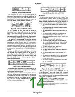
EEPROM
The ADM1026 has 8 kB of non−volatile, electrically
erasable, programmable read−only memory (EEPROM)
from register Addresses 8000h to 9FFFh. This may be used
for permanent storage of data that is not lost when the
Any or all of the interrupt status bits can be masked by
appropriate programming of the interrupt mask registers.
http://onsemi.com
10

 ONSEMI [ ONSEMI ]