74HC74
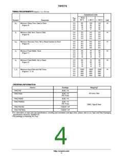
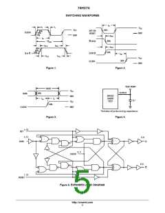
TIMING REQUIREMENTS (Input t = t = 6.0 ns)
r
f
Guaranteed Limit
– 55 to
V
CC
25_C
80
35
16
14
(V)
v 85_C v 125_C
Symbol
Parameter
Unit
t
ns
Minimum Setup Time, Data to Clock
(Figure 3)
2.0
3.0
4.5
6.0
100
45
120
55
su
20
24
17
20
t
3.0
3.0
3.0
3.0
ns
ns
ns
ns
ns
Minimum Hold Time, Clock to Data
(Figure 3)
2.0
3.0
4.5
6.0
3.0
3.0
3.0
3.0
3.0
3.0
3.0
3.0
h
t
Minimum Recovery Time, Set or Reset Inactive to Clock
(Figure 2)
2.0
3.0
4.5
6.0
8.0
8.0
8.0
8.0
8.0
8.0
8.0
8.0
8.0
8.0
8.0
8.0
rec
t
Minimum Pulse Width, Clock
(Figure 1)
2.0
3.0
4.5
6.0
60
25
12
10
75
30
15
13
90
40
18
15
w
t
Minimum Pulse Width, Set or Reset
(Figure 2)
2.0
3.0
4.5
6.0
60
25
12
10
75
30
15
13
90
40
18
15
w
t , t
r
Maximum Input Rise and Fall Times
(Figures 1, 2, 3)
2.0
3.0
4.5
6.0
1000
800
500
400
1000
800
500
400
1000
800
500
400
f
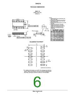
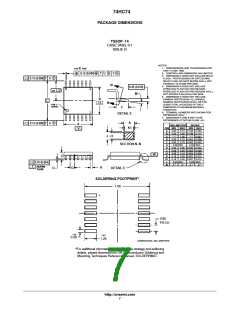
ORDERING INFORMATION
Device
†
Package
Shipping
74HC74D
SOIC−14
55 Units / Rail
74HC74DG
SOIC−14
(Pb−Free)
74HC74DR2
SOIC−14
74HC74DR2G
SOIC−14
(Pb−Free)
2500 / Tape & Reel
74HC74DTR2
TSSOP−14*
TSSOP−14*
74HC74DTR2G
†For information on tape and reel specifications, including part orientation and tape sizes, please refer to our Tape and Reel Packaging
Specifications Brochure, BRD8011/D.
*This package is inherently Pb−Free.
http://onsemi.com
4

 ONSEMI [ ONSEMI ]