74HC74
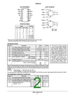
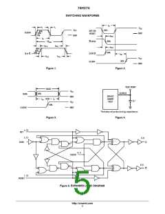
PIN ASSIGNMENT
LOGIC DIAGRAM
1
RESET 1
DATA 1
1
2
14
13 RESET 2
12
V
RESET 1
CC
5
6
2
3
DATA 1
Q1
Q1
3
4
CLOCK 1
SET 1
DATA 2
CLOCK 1
11 CLOCK 2
10 SET 2
4
Q1
Q1
5
6
7
SET 1
9
8
Q2
Q2
13
RESET 2
GND
9
8
12
11
DATA 2
Q2
Q2
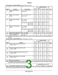
FUNCTION TABLE
CLOCK 2
Inputs
Outputs
10
Set Reset Clock Data
Q
Q
SET 2
PIN 14 = V
CC
PIN 7 = GND
L
H
L
H
H
H
H
H
H
L
L
H
H
H
H
H
X
X
X
X
X
X
H
L
X
X
X
H
L
H*
H
L
L
H
H*
L
H
L
H
No Change
No Change
No Change
*Both outputs will remain high as long as Set and Reset are low, but the output
states are unpredictable if Set and Reset go high simultaneously.
MAXIMUM RATINGS
Symbol
Parameter
DC Supply Voltage (Referenced to GND)
DC Input Voltage (Referenced to GND)
DC Output Voltage (Referenced to GND)
DC Input Current, per Pin
Value
Unit
V
This device contains protection
circuitry to guard against damage
due to high static voltages or electric
fields. However, precautions must
be taken to avoid applications of any
voltage higher than maximum rated
voltages to this high−impedance cir-
V
– 0.5 to + 7.0
CC
V
in
– 0.5 to V + 0.5
V
CC
V
out
– 0.5 to V + 0.5
V
CC
I
±20
±25
±50
mA
mA
mA
mW
in
I
DC Output Current, per Pin
out
CC
cuit. For proper operation, V and
in
I
DC Supply Current, V and GND Pins
CC
V
out
should be constrained to the
P
Power Dissipation in Still Air,
SOIC Package†
TSSOP Package†
500
450
range GND v (V or V ) v V
.
D
in
out
CC
Unused inputs must always be
tied to an appropriate logic voltage
T
stg
Storage Temperature
– 65 to + 150
_C
_C
level (e.g., either GND or V ).
CC
T
Lead Temperature, 1 mm from Case for 10 Seconds
(SOIC or TSSOP Package)
L
Unused outputs must be left open.
260
300
Stresses exceeding Maximum Ratings may damage the device. Maximum Ratings are stress
ratings only. Functional operation above the Recommended Operating Conditions is not implied.
Extended exposure to stresses above the Recommended Operating Conditions may affect device
reliability.
†Derating — SOIC Package: – 7 mW/_C from 65_ to 125_C
TSSOP Package: − 6.1 mW/_C from 65_ to 125_C
For high frequency or heavy load considerations, see Chapter 2 of the ON Semiconductor High−Speed CMOS Data Book (DL129/D).
RECOMMENDED OPERATING CONDITIONS
Symbol
Parameter
Min
2.0
0
Max
Unit
V
V
DC Supply Voltage (Referenced to GND)
DC Input Voltage, Output Voltage (Referenced to GND)
Operating Temperature, All Package Types
6.0
CC
V , V
in out
V
V
CC
T
A
– 55
+ 125
_C
ns
t , t
Input Rise and Fall Time
(Figures 1, 2, 3)
V
V
V
V
= 2.0 V
= 3.0 V
= 4.5 V
= 6.0 V
0
0
0
0
1000
600
500
400
r
f
CC
CC
CC
CC
http://onsemi.com
2

 ONSEMI [ ONSEMI ]