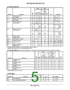
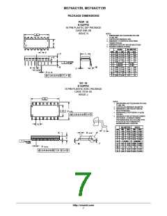
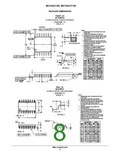
MC74AC139, MC74ACT139
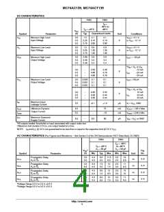
MAXIMUM RATINGS*
Symbol
Parameter
Value
Unit
V
V
V
V
DC Supply Voltage (Referenced to GND)
−0.5 to +7.0
CC
DC Input Voltage (Referenced to GND)
DC Output Voltage (Referenced to GND)
DC Input Current, per Pin
−0.5 to V +0.5
V
IN
CC
−0.5 to V +0.5
V
OUT
CC
I
I
I
±20
±50
mA
mA
mA
°C
IN
DC Output Sink/Source Current, per Pin
OUT
CC
DC V or GND Current per Output Pin
±50
CC
T
stg
Storage Temperature
−65 to +150
*Maximum Ratings are those values beyond which damage to the device may occur. Functional operation should be restricted to the Recom-
mended Operating Conditions.
RECOMMENDED OPERATING CONDITIONS
Symbol
Parameter
Min
2.0
4.5
0
Typ
5.0
5.0
−
Max
6.0
Unit
′AC
V
V
Supply Voltage
V
V
CC
′ACT
5.5
, V
OUT
DC Input Voltage, Output Voltage (Ref. to GND)
V
CC
IN
V
CC
V
CC
V
CC
V
CC
V
CC
@ 3.0 V
@ 4.5 V
@ 5.5 V
@ 4.5 V
@ 5.5 V
−
150
40
25
10
8.0
−
−
Input Rise and Fall Time (Note 1)
′AC Devices except Schmitt Inputs
−
−
−
−
−
ns/V
t , t
r
f
−
−
Input Rise and Fall Time (Note 2)
′ACT Devices except Schmitt Inputs
t , t
ns/V
r
f
−
T
J
Junction Temperature (PDIP)
Operating Ambient Temperature Range
Output Current − High
−
140
85
°C
°C
T
A
−40
−
25
−
I
I
−24
24
mA
mA
OH
OL
Output Current − Low
−
−
1. V from 30% to 70% V ; see individual Data Sheets for devices that differ from the typical input rise and fall times.
IN
CC
2. V from 0.8 V to 2.0 V; see individual Data Sheets for devices that differ from the typical input rise and fall times.
IN
http://onsemi.com
3

 ONSEMI [ ONSEMI ]